Check patentability & draft patents in minutes with Patsnap Eureka AI!

GaN-based inverted HEMT device structure and manufacturing method thereof

A device structure and flip-chip technology, which is applied in semiconductor/solid-state device manufacturing, electric solid-state devices, semiconductor devices, etc., can solve the problems of poor heat dissipation, low breakdown voltage, and low effective use area of ​​epitaxial wafers, etc., to achieve easy heat dissipation, Effects of improving high-voltage resistance characteristics and improving effective utilization

Active Publication Date: 2015-11-18
SOUTH CHINA UNIV OF TECH
View PDF5 Cites 2 Cited by
  • Summary
  • Abstract
  • Description
  • Claims
  • Application Information

AI Technical Summary

Problems solved by technology

[0004] Aiming at the problems of poor heat dissipation, low breakdown voltage and low effective use area of ​​epitaxial wafers in existing GaN-based HEMT devices, the present invention proposes a GaN-based flip-chip high electron mobility transistor structure. The epitaxial layer of the transistor passes through the metal electrode and the heat-dissipating substrate. connection, good heat dissipation performance; the area of ​​the gate electrode pad is originally larger than the gate electrode itself, which can homogenize the distribution of electric field intensity and improve the high-voltage resistance characteristics of the device; in addition, the electrode pad is above the electrode, and the utilization rate of the epitaxial layer is high

Method used


Image

  • GaN-based inverted HEMT device structure and manufacturing method thereof
  • GaN-based inverted HEMT device structure and manufacturing method thereof
  • GaN-based inverted HEMT device structure and manufacturing method thereof

Examples


Embodiment 1

[0045] Example 1, Fabrication of GaN-based flip-chip HEMT

[0046] Such as image 3 As shown, the preparation method steps are as follows:

[0047] (1) Growing a high electron mobility transistor epitaxial layer on a substrate according to the prior art.

[0048] (2) Put the sample of step (1) into boiling acetone for 5 minutes, then into boiling ethanol for 5 minutes, then rinse with deionized water for 5 minutes, and then dry with nitrogen;

[0049] (3) Prepare a mask on the sample surface described in step (2), etch the GaN by inductively coupled plasma (ICP) etching technology, etch the two-dimensional electron gas (2DEG), isolate the mesa, and then remove the mask ;

[0050] (4) After cleaning the surface of the sample described in step (3), deposit Ti / Al / Ti / Au alloy with a thickness of 10 / 300 / 100 / 500nm, and then prepare source and drain electrodes by photolithography technology, and obtain source and drain electrodes after annealing. Leakage ohmic contact;

[0051] (5) After cle...

Embodiment 2

[0060] Example 2, Fabrication of GaN-based flip-chip HEMT

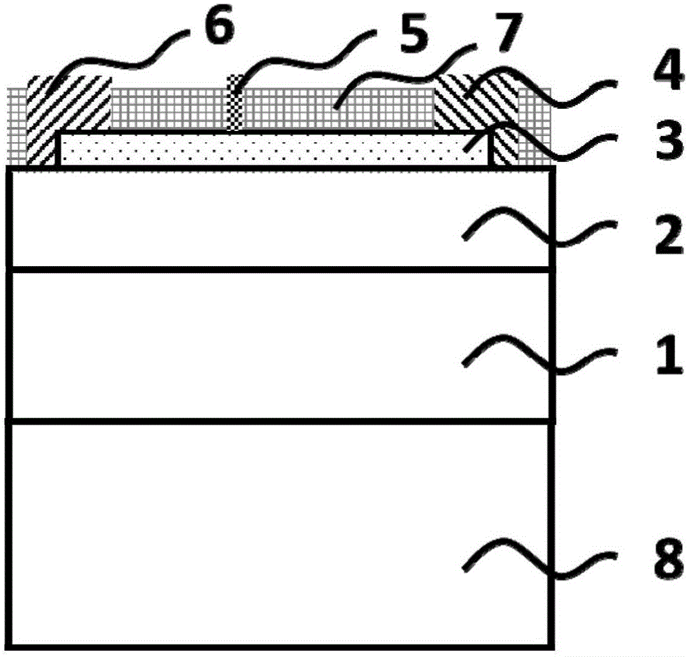
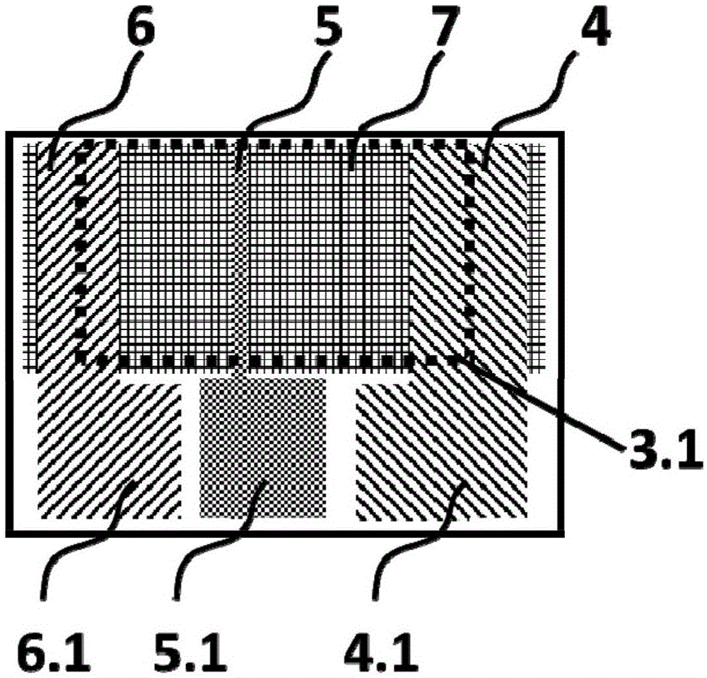
[0061] Such as image 3 As shown, the thin film transistors from bottom to top are 8 substrates, 5.1 gate electrode pads, 5 gate electrodes, 7 insulating dielectric films, 4 drain electrodes, 6 source electrodes, 3AlGaN barrier layers, 2GaN buffer layers, 9 conductive Through holes, 4.1 floor click pads and 6.1 source electrode pads.

[0062] The basic steps of Example 2 are the same as that of Example 1, except that:

[0063] Step (10) completely remove the original substrate of the sample.

[0064] The present invention addresses the problems of poor heat dissipation, low breakdown voltage, and low epitaxial layer utilization of existing transistors, and proposes a flip-chip HEMT structure. After the electrodes are prepared from the epitaxial wafer, it is bonded to the substrate, and then the original liner is thinned and removed. At the bottom, the source and drain electrodes are electrically connected to the pads throu...


PUM


Abstract

The invention relates to a GaN-based inverted HEMT device structure and a manufacturing method thereof. The GaN-based inverted HEMT device structure comprises a substrate, electrode welding pads, electrodes, an insulating dielectric film, an epitaxial layer and conductive through holes, wherein the epitaxial layer comprises a GaN buffer layer and an AlGaN barrier layer, one end of the gate electrode passes through the insulating dielectric film and is connected with the gate electrode welding pad, the other end of the gate electrode is connected with the AlGaN barrier layer of the epitaxial layer, and the epitaxial layer is adhered with the substrate through the gate electrode welding pad; and the substrate, the gate electrode welding pad, the insulating dielectric film, the AlGaN barrier layer and the GaN buffer layer are arranged from bottom to top. According to the GaN-based inverted HEMT device structure, an epitaxial wafer of an HEMT device is connected with the radiating substrate through the gate electrode welding pad, the radiating performance is improved significantly. In addition, the source, drain and gate electrode welding pads are arranged on the epitaxial layer without etching useless part of the epitaxial layer away, and the effective utilization rate of the epitaxial layer is increased. The invention further provides the manufacturing method of the GaN-based inverted HEMT device structure.

Description

technical field [0001] The invention relates to the technical field of semiconductor microelectronics, in particular to a GaN / AlGaN-based flip-chip transistor structure and a preparation method thereof. Background technique [0002] As a third-generation semiconductor material, GaN has a higher band gap, a greater electron saturation drift velocity, a stronger near-breakdown electric field, higher thermal conductivity, and thermal stability. GaN-based nitride semiconductor materials also have great spontaneous and piezoelectric polarization characteristics. The high electron mobility transistor prepared by using this characteristic is a field-effect semiconductor device, which is widely used in high-frequency amplifier devices or high-power switching devices. field. [0003] The general structure of GaN-based high electron mobility transistor (HEMT) is substrate, buffer layer, barrier layer, dielectric film and electrode. Conventional HEMT substrates have low thermal condu...

Claims


Application Information

Patent Timeline
IPC IPC(8): H01L23/488H01L23/367H01L29/778H01L21/335H01L21/60
Inventor 徐明升周泉斌王洪
Owner SOUTH CHINA UNIV OF TECH
Features
  • R&D
  • Intellectual Property
  • Life Sciences
  • Materials
  • Tech Scout
  • Unparalleled Data Quality
  • Higher Quality Content
  • 60% Fewer Hallucinations
Learn More