Preparation method, based on solution method, of polycrystalline solar cell

A solar cell, solution method technology, applied in nanotechnology, circuits, photovoltaic power generation and other directions for materials and surface science, can solve the problems of low conversion efficiency of black silicon cells, achieve low reflectivity, low solution cost, temperature low effect

Active Publication Date: 2015-11-18
江西汉可泛半导体技术有限公司
View PDF4 Cites 21 Cited by
  • Summary
  • Abstract
  • Description
  • Claims
  • Application Information

AI Technical Summary

Problems solved by technology

However, the conversion efficiency of black silicon cells is generally low, even lower than conventional textured solar cells without black silicon anti-reflection structures

Method used


Image

  • Preparation method, based on solution method, of polycrystalline solar cell
  • Preparation method, based on solution method, of polycrystalline solar cell
  • Preparation method, based on solution method, of polycrystalline solar cell

Examples


preparation example Construction

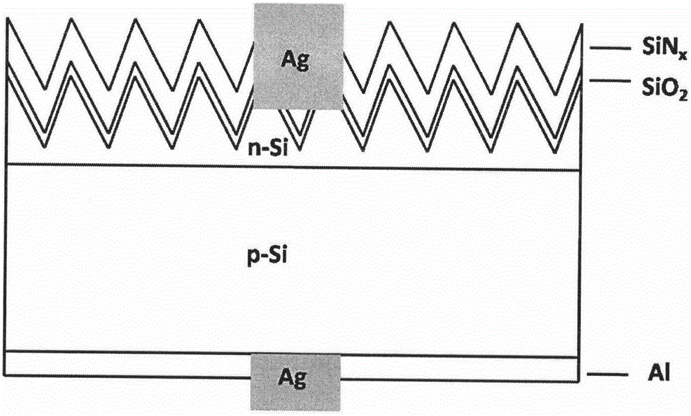
[0026] In order to control the preparation cost of black silicon and improve the conversion efficiency of black silicon cells, an embodiment of the present invention provides a method for preparing polycrystalline solar cells based on a solution method, including:

[0027] (1) cleaning the surface of the silicon wafer;

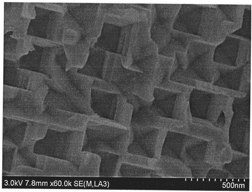
[0028] (2) Deposit silver nanoparticles on the surface of the silicon wafer, and catalyze and corrode the black silicon nanoporous structure;

[0029] (3) Cleaning the prepared black silicon with NSR and hydrogen peroxide solution to form an inverted pyramid anti-reflection structure on the surface of the silicon wafer;

[0030] (4) After cleaning before diffusion, diffusion is performed in a diffusion furnace to form a PN junction;

[0031] (5) Then wet etching process is used to etch the back junction and edge junction of the diffused silicon wafer, and remove the surface phosphosilicate glass and the diffusion dead layer;

[0032] (6) The silicon oxide in...

Embodiment 1

[0038] (1) In the volume ratio HF (40%): HNO 3 (70%): H 2 Etching was carried out in a solution of O=1:3:2, the time was 3 min, and the temperature was room temperature. The concentration of NaOH solution used to remove the porous silicon is 1%, the time is 30 s, and the temperature is room temperature.

[0039] (2) Deposit a layer of silver nanoparticles on the surface of the silicon wafer immersed in the solution, 0.002MAgNO 3 +4MHF, response time 50s;

[0040] (3) Immerse the silicon wafer deposited with silver nanoparticles in the solution for corrosion, 0.3MH 2 o 2 +1.5MHF to obtain nano-hole structure, the reaction time is 180s. ;

[0041] (4) immerse the etched black silicon wafer in the solution for cleaning, remove residual silver nanoparticles, H 2 o 2 : NH 4 OH=1:3, the reaction time is 180s;

[0042] (5) Immersing the prepared black silicon into the solution for etching to prepare an inverted pyramid black silicon structure. Utilizing the anisotropic cor...

Embodiment 2

[0045] Prepare a solar cell with the structure described in Example 1:

[0046] Pre-cleaned in HCl and HF solutions, the N-type emitter in the PN junction is made of POCl 3 It is obtained by diffusion, the diffusion temperature is 825°C, and the rear resistance of diffusion is 70Ω / sq; the wet etching process mainly uses HF and HNO 3 solution to etch the back junction and edge junction, and then use dilute HF solution to remove the surface phosphosilicate glass; in HNO 3 (69%): H 2 O=1:3 solution in a water bath for 30 minutes at a temperature of 80°C to prepare a very thin inner layer of silicon oxide passivation layer; then PECVD deposited 85nm SiN x , deposited onto the black silicon emitter surface. When screen-printing electrodes, the back side is made of aluminum paste, and the front and back grid electrodes are made of silver paste. Finally, a rapid heat treatment is carried out in a chain sintering furnace.

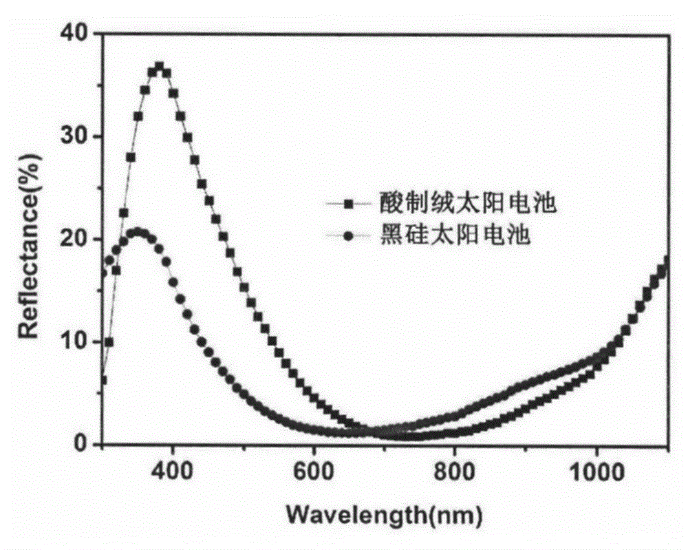
[0047] The result of the embodiment: compared with the c...


PUM

PropertyMeasurementUnit
pore sizeaaaaaaaaaa
thicknessaaaaaaaaaa
thicknessaaaaaaaaaa

Abstract

The invention discloses a preparation method, based on a solution method, of a polycrystalline solar cell. The method includes the steps: (1) preparing a black silicon structure of the surface of a silicon oxide through a metal assisted chemical etching (MACE) technology; (2) performing optimized processing for the black silicon structure through a nano-structure rebuilding (NSR) solution so that an uniform reverse pyramid structure is formed; (3) changing the sheet resistance after diffusion and the thickness of a silicon nitride passive film on the nano-structure; and (4) forming a silicon oxide/silicon nitride dual-layer passive structure through liquid phase processing and PECVD. The prepared reverse pyramid anti-reflection structure has a better anti-reflection effect compared with a worm type structure formed by acid texturing, and is easier to passivate compared with a nano-black silicon structure, and is an ideal black silicon anti-reflection structure. The preparation method can prepare a polycrystalline solar cell that is low in reflectivity and high in conversion efficiency. Compared with a conventional cell process, the process of the method is simple, only adopts liquid phase processing, is low in cost, and is suitable for industrialized batch production.

Description

technical field [0001] The invention relates to a method for preparing a polycrystalline solar cell based on a solution method. The invention can prepare nanometer inverted pyramid polycrystalline solar cells with low reflectivity and high conversion efficiency, and is suitable for the technical field of solar photovoltaic cells. Background technique [0002] With its advantages in conversion efficiency and mass production cost, crystalline silicon solar cells maintain a high market share in the photovoltaic industry and continue to develop. In order to further strengthen the competitiveness of crystalline silicon solar cells, improving the conversion efficiency has always been the direction that researchers are committed to. As a technical means to effectively improve the conversion efficiency of crystalline silicon solar cells, black silicon technology has been extensively studied. [0003] The development of black silicon technology can be roughly divided into three sta...

Claims


Application Information

Patent Timeline
Patent Type & Authority Applications(China)
IPC IPC(8): H01L31/18B82Y40/00B82Y30/00
CPCB82Y30/00B82Y40/00H01L31/18H01L31/182Y02E10/546Y02P70/50
Inventor 沈鸿烈蒋晔蒲天
Owner 江西汉可泛半导体技术有限公司
Why Eureka
Try Eureka