4H-SiC metal semiconductor field effect transistor having partial sinking channel

A field-effect transistor and metal-semiconductor technology, which is applied in the field of 4H-SiC metal-semiconductor field-effect transistors, can solve problems such as device breakdown voltage suppression and drop

Active Publication Date: 2015-12-02
XIDIAN UNIV
View PDF2 Cites 2 Cited by
  • Summary
  • Abstract
  • Description
  • Claims
  • Application Information

AI Technical Summary

Problems solved by technology

[0004] Compared with the traditional structure, although the saturation leakage current of the double-recessed 4H-SiCMESFET structure has been improved due to

Method used


Image

  • 4H-SiC metal semiconductor field effect transistor having partial sinking channel
  • 4H-SiC metal semiconductor field effect transistor having partial sinking channel

Examples


Embodiment 1

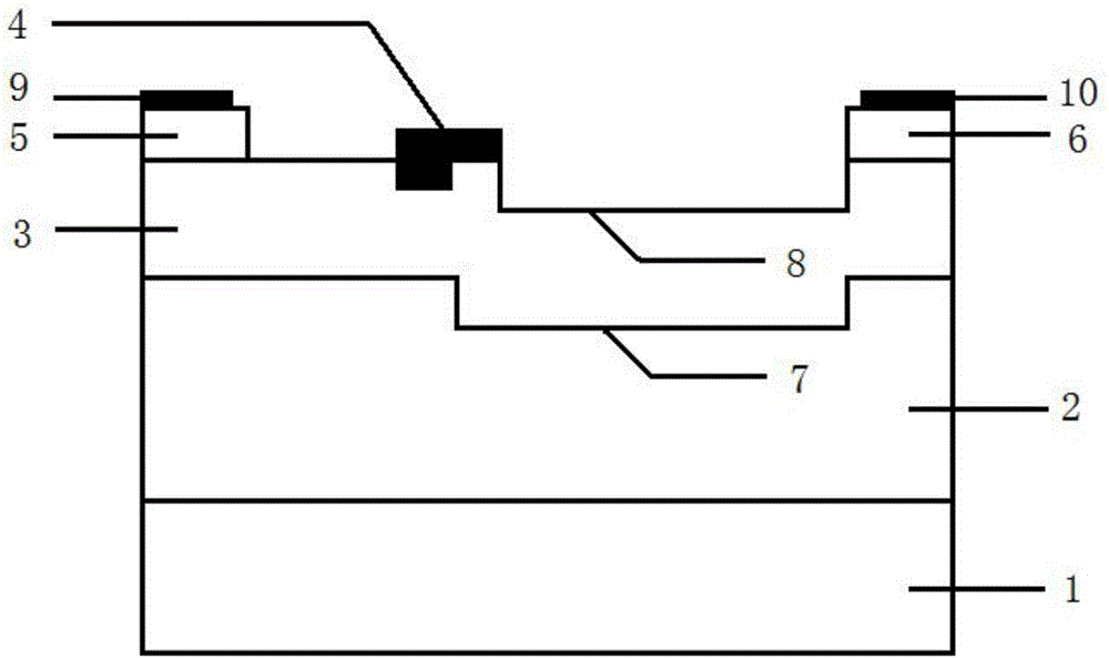
[0035] A 4H-SiC metal-semiconductor field-effect transistor with a recessed gate-drain buffer layer thickness and a recessed gate-drain drift region thickness of 0.1 μm is manufactured.

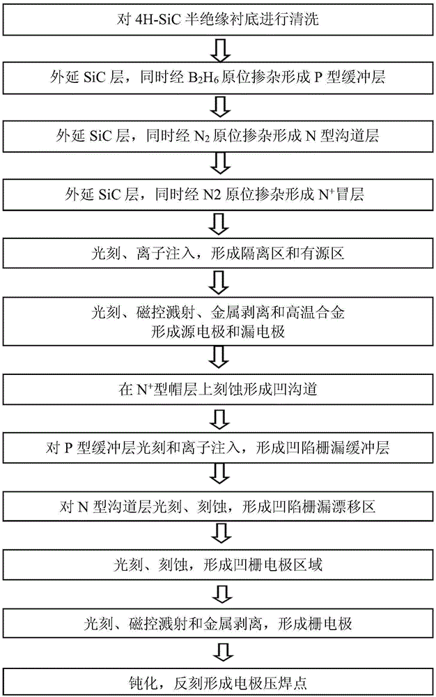
[0036] The manufacturing steps of this embodiment are as follows:

[0037] Step 1: cleaning the 4H-SiC semi-insulating substrate 1 to remove surface pollutants.

[0038] (1.1) Carefully wash the substrate twice with a cotton ball dipped in methanol to remove SiC particles of various sizes on the surface;

[0039] (1.2) Place the substrate in H 2 SO4 :HNO 3 = Ultrasound for 5 minutes in 1:1;

[0040] (1.3) Put the substrate in 1# cleaning solution (NaOH:H 2 o 2 :H 2 O=1:2:5), boiled for 5 minutes, rinsed with deionized water for 5 minutes, and then put into 2# cleaning solution (HCl:H 2 o 2 :H 2 O=1:2:7) and boiled for 5 minutes. Finally rinsed with deionized water and rinsed with N 2 Blow dry and set aside.

[0041] Step 2: epitaxially grow a SiC layer on the surface of the 4H-SiC...

Embodiment 2

[0085] A 4H-SiC metal-semiconductor field-effect transistor with a recessed gate-drain buffer layer thickness and a recessed gate-drain drift region thickness of 0.08 μm was fabricated.

[0086] Step 8: Photoetching and ion implanting the P-type buffer layer 2 to form a recessed gate-drain buffer layer 7 .

[0087] (8.1) Use positive photoresist, glue coating speed: 3000R / min, glue thickness > 2μm to ensure that it can play a good blocking role in the subsequent isolation injection;

[0088] (8.2) After gluing is completed, pre-bake in an oven at 90°C for 90 seconds, use a stepped buffer layer photolithography plate for about 35 seconds of UV exposure, and then develop in a special developer (tetramethylammonium hydroxide: water = 1:3) 60 seconds, then post-bake in an oven at 100°C for 3 minutes;

[0089] (8.3) Perform nitrogen ion implantation, the implantation condition is 240keV / 2×10 12 cm -2 , the temperature is 400°C. After the injection is completed, use acetone + ul...

Embodiment 3

[0097] A 4H-SiC metal-semiconductor field-effect transistor with a recessed gate-drain buffer layer thickness and a recessed gate-drain drift region thickness of 0.11 μm was fabricated.

[0098] Step 8: Photoetching and ion implanting the P-type buffer layer 2 to form a recessed gate-drain buffer layer 7 .

[0099] (8.1) Use positive photoresist, glue coating speed: 3000R / min, glue thickness > 2μm to ensure that it can play a good blocking role in the subsequent isolation injection;

[0100] (8.2) After gluing is completed, pre-bake in an oven at 90°C for 90 seconds, use a stepped buffer layer photolithography plate for about 35 seconds of UV exposure, and then develop in a special developer (tetramethylammonium hydroxide: water = 1:3) 60 seconds, then post-bake in an oven at 100°C for 3 minutes;

[0101] (8.3) Perform nitrogen ion implantation, the implantation condition is 270keV / 2×10 12 cm -2 , the temperature is 400°C. After the injection is completed, use acetone + ul...


PUM

PropertyMeasurementUnit
Lengthaaaaaaaaaa
Depthaaaaaaaaaa

Abstract

The invention discloses a 4H-SiC metal semiconductor field effect transistor having a partial sinking channel. The 4H-SiC metal semiconductor field effect transistor having a partial sinking channel, from the bottom to the top, comprises a 4H-SiC half insulation substrate, a P type buffer layer, and an N type channel layer; the N type channel layer surface is provided with a source electrode cap layer and a drain electrode cap layer; the surfaces of the source electrode cap layer and the drain electrode cap layer are provided with a source electrode and a drain electrode; a grating electrode is formed above the N type channel layer and close to one side of the source electrode cap layer; part of the grating electrode close to the source electrode cap layer concaves downwardly to form a concave grating structure; a concave grating drain drifting area is formed between the grating electrode and the drain electrode cap layer; a concave grating drain buffer layer is formed on the upper end surface of a P buffer layer and close to the portion between the drain electrode cap layer and the concave grating drain side; and the concave depth of the concave grating drain drifting area is identical to that of the concave grating drain buffer layer. The 4H-SIC metal semiconductor field effect transistor having a partial sinking channel has advantages that the drain electrode is big in output current, the breakdown voltage is high and frequency characteristic is good.

Description

technical field [0001] The invention relates to the technical field of field effect transistors, in particular to a 4H-SiC metal semiconductor field effect transistor with a partially sunken channel. Background technique [0002] SiC materials have excellent electrical properties, including wide bandgap [(2.3~3.3)eV], high breakdown electric field [(0.8~3.0)×10 6 V / cm], high saturation drift velocity (2×10 7 V / cm) and high thermal conductivity (4.9Wcm -1 K -1 ), these characteristics can make SiC devices work under special conditions of high temperature, high power and high frequency. A notable feature of SiC materials is homogeneous polytype. Among all SiC polytypes, 4H-SiC with hexagonal close-packed wurtzite structure has received a high degree of attention, because the electron mobility of 4H-SiC structure It is about twice as much as 6H-SiC. Therefore, 4H-SiC materials occupy a dominant position in high-frequency high-power devices, especially metal-semiconductor f...

Claims


Application Information

Patent Timeline
IPC IPC(8): H01L29/812H01L29/06H01L29/10H01L29/24H01L21/338
CPCH01L29/0684H01L29/1029H01L29/24H01L29/66848H01L29/8128
Inventor 贾护军罗烨辉马培苗杨志辉
Owner XIDIAN UNIV
Why Eureka
Try Eureka