Wafer-level packaging method based on silicon molecular sieve and polytetrafluoroethylene composite film
A polytetrafluoroethylene, wafer-level packaging technology, applied in the process of producing decorative surface effects, decorative arts, measuring devices, etc., to achieve the effect of improving packaging efficiency and reducing packaging costs
- Summary
- Abstract
- Description
- Claims
- Application Information
AI Technical Summary
Problems solved by technology
Method used
Image

Examples
preparation example Construction
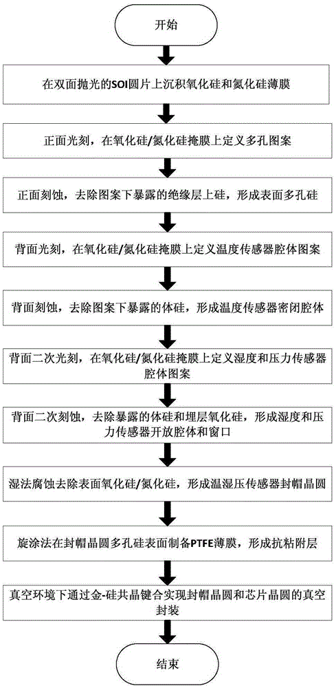
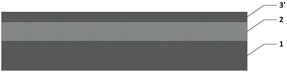
[0029] The method of the invention consists of three parts: preparation of silicon molecular sieve, formation of encapsulation cavity and gold-silicon eutectic bonding. Among them, silicon molecular sieves are prepared by deep hole etching, and the size of the particles that can pass through is selected by controlling the pore size of the molecular sieve, which plays a role in blocking large molecules and passing small molecules. In order to solve the problem that the surface of the silicon molecular sieve is easy to adhere to dust, water vapor, oil and other chemical substances, thereby causing the clogging of the molecular sieve, the present invention modifies the surface of the silicon molecular sieve, that is, prepares a layer of hydrophobic and oleophobic polymer organic polymer film - Polytetrafluoroethylene film (PTFE). The PTFE film not only has extremely small surface tension and excellent corrosion resistance, but also has a simple preparation process and can be conv...
PUM
| Property | Measurement | Unit |
|---|---|---|
| Thickness | aaaaa | aaaaa |
Abstract
Description
Claims
Application Information
 - Generate Ideas
- Intellectual Property
- Life Sciences
- Materials
- Tech Scout
- Unparalleled Data Quality
- Higher Quality Content
- 60% Fewer Hallucinations
Browse by: Latest US Patents, China's latest patents, Technical Efficacy Thesaurus, Application Domain, Technology Topic, Popular Technical Reports.
© 2025 PatSnap. All rights reserved.Legal|Privacy policy|Modern Slavery Act Transparency Statement|Sitemap|About US| Contact US: help@patsnap.com