Preparation method for nanoporous silicon
A nanoporous, industrial silicon technology, applied in nanotechnology, nanotechnology, chemical instruments and methods, etc., can solve the problems of uneven porous silicon pores, cumbersome operation process, and high equipment requirements, and achieve uniform pore size and short process flow , the effect of low equipment requirements
- Summary
- Abstract
- Description
- Claims
- Application Information
AI Technical Summary
Problems solved by technology
Method used
Image
Examples
Embodiment 1
[0039] Step 1. Weigh 6.6g of magnesium powder and 3g of industrial silicon powder, mix them evenly and put them in a quartz tube, then use a molecular pump to evacuate the quartz tube and seal it.
[0040] Step 2. Put the quartz tube into the vertical pulling furnace, raise the temperature to 700 °C at a rate of 5 °C / min, and keep it warm for 1 hour, then cool to room temperature with the furnace, open the quartz tube, and take out the Mg 2 Si-Mg alloy and grind it into powder.
[0041] Step 3, weigh 3g of Mg 2 Si-Mg alloy powder and 9g of ZnCl 2 , mixed evenly, placed in a corundum crucible, placed in a tube furnace, and fed with Ar gas, then heated to 300°C at a rate of 5°C / min, kept for 10h, and dealloyed.
[0042] Step 4. Soak the product of step 3 in 10% hydrochloric acid for 5 hours, then centrifuge at 8000r / min for 5 minutes, filter until the solution is neutral, and dry it in vacuum at 60°C in a drying oven.
Embodiment 2
[0044] The difference between this embodiment and Example 1 is that in step 1, 7.5g of magnesium powder and 3g of industrial silicon powder are weighed, and 15g of ZnCl in step 3 2 , others are the same as in Example 1.
Embodiment 3
[0046] The difference between this embodiment and Example 1 is that in step 3, 12g of AlCl is weighed 3 , others are the same as in Example 1.
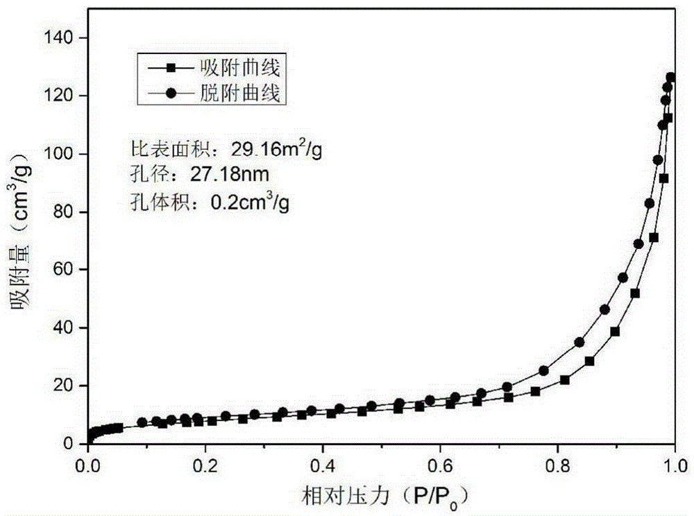
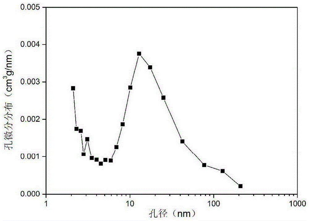
[0047] figure 1 , figure 2 It is the nitrogen adsorption-desorption curve and pore size distribution diagram of the nanoporous silicon of the sample in Example 1.
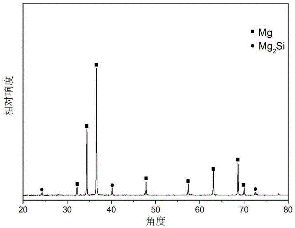
[0048] image 3 , Figure 4 Be the XRD diffraction pattern of embodiment 3 samples.
[0049] Figure 6 It is the nanoporous silicon SEM scanning spectrum of the sample in Example 2.
PUM
 Abstract
Description
Claims
Application Information


