A kind of micro-channel type incident window and its manufacturing method

A manufacturing method and incident window technology, which are applied in the field of photoelectric detection, can solve the problems of difficult preparation, complex structure of photoelectric detectors, high cost, etc., and achieve the effects of easy preparation, simple structure and strong applicability

Active Publication Date: 2017-09-22
XI'AN INST OF OPTICS & FINE MECHANICS - CHINESE ACAD OF SCI
View PDF4 Cites 0 Cited by
  • Summary
  • Abstract
  • Description
  • Claims
  • Application Information

AI Technical Summary

Problems solved by technology

[0012] The purpose of the present invention is to provide a micro-channel type entrance window and its manufacturing method. The entrance window has the functions of photoelectric emission and electron multiplication, which can effectively solve the shortcomings of existing photodetectors, such as complex structure, difficult preparation, and high cost. At the same time, the honeycomb structure of the incident window is used to increase the effective area of ​​the photocathode, increase the probability of incident photons being absorbed by the photocathode, and then improve the quantum efficiency of the photocathode

Method used


Image

  • A kind of micro-channel type incident window and its manufacturing method
  • A kind of micro-channel type incident window and its manufacturing method
  • A kind of micro-channel type incident window and its manufacturing method

Examples


Embodiment 1

[0053] A metal antimony cathode sensitive to X-rays is prepared by atomic layer deposition technology alone.

[0054] Step 1) ultrasonically clean the incident window in acetone, alcohol and deionized water for 10 minutes respectively;

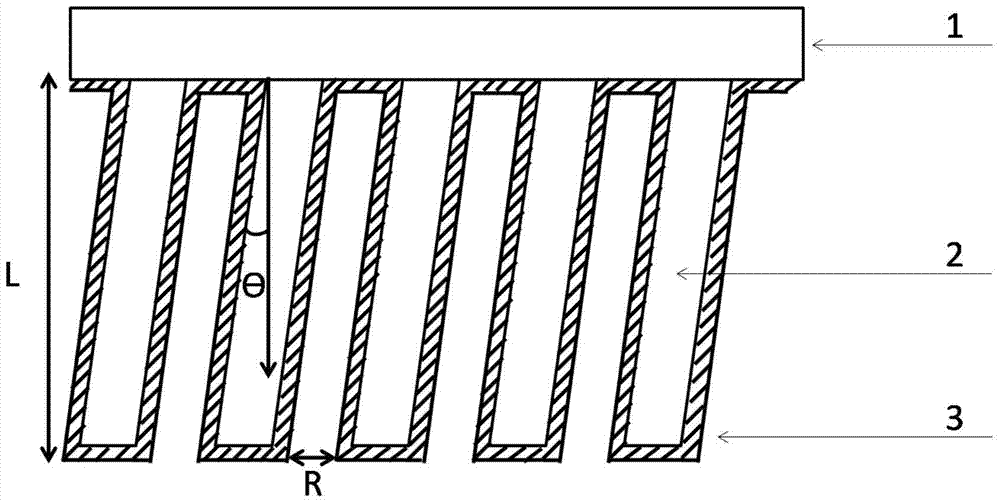
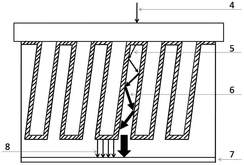
[0055] Step 2) Fabricate a honeycomb structure on the entrance window by adopting the process of ordinary photolithography first and then ion beam etching or adopting the process of ordinary photolithography first and then acid etching;

[0056] Step 3) Perform high-temperature annealing on the entrance window etched into a honeycomb structure and then clean the entrance window again; (the cleaning process is the same as step 1)

[0057] Step 4) Put the above incident window into the atomic layer deposition system, and use the two precursor compounds of antimony to react to form a metal antimony film on the incident window at a temperature of 100 degrees. The thickness of the antimony film is displayed by a film thickness monitor , the genera...

Embodiment 2

[0059] A tellurium-cesium cathode sensitive to ultraviolet light is prepared by molecular beam epitaxy alone.

[0060] Step 1) The incident window was ultrasonically cleaned in acetone, alcohol and deionized water for 10 minutes each in sequence.

[0061] Step 2) Fabricate a honeycomb structure on the entrance window by adopting the process of ordinary photolithography first and then ion beam etching or adopting the process of ordinary photolithography first and then acid etching;

[0062] Step 3) Perform high-temperature annealing on the entrance window etched into a honeycomb structure and then clean the entrance window again; (the cleaning process is the same as step 1)

[0063] Step 4) Transfer the incident window to a vacuum system, grow a tellurium film on the incident window at room temperature, and observe the thickness of the tellurium film with a film thickness monitor, generally 20 nanometers in thickness;

[0064] Step 5) Raise the temperature of the vacuum chambe...

Embodiment 3

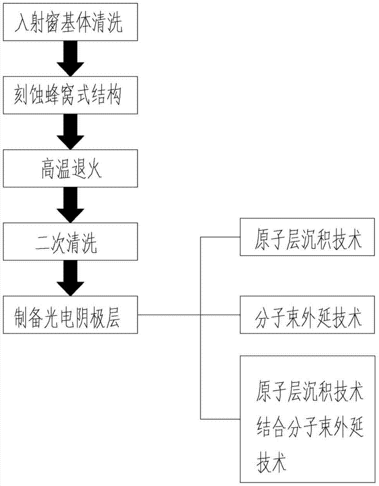
[0067] Such as image 3 Shown: Alkali metal photocathode is prepared by combining atomic layer deposition technology and molecular beam epitaxy technology.

[0068] Step 1) The incident window was ultrasonically cleaned in acetone, alcohol and deionized water for 10 minutes each in sequence.

[0069] Step 2) Fabricate a honeycomb structure on the entrance window by adopting the process of ordinary photolithography first and then ion beam etching or adopting the process of ordinary photolithography first and then acid etching;

[0070] Step 3) Perform high-temperature annealing on the entrance window etched into a honeycomb structure and then clean the entrance window again; (the cleaning process is the same as step 1)

[0071] Step 4) On the basis of the above-mentioned incident window substrate, a metal antimony (Sb) film is deposited on the surface of the substrate and the inner wall of the through hole by atomic layer deposition technology, and the thickness of the antimon...


PUM


Abstract

The invention belongs to the technical field of photoelectric detection, and in particular relates to a micro-channel type incident window and a production method thereof. The micro-channel type incident window comprises an incident window substrate, wherein the incident window substrate is of the honeycomb structure including a plurality of through hole, the through holes are formed by common photoetching and ion beam etching or acid corrosion technology; and photoelectric cathode layers are deposited on the surface of the incident window substrate and in the plurality of through holes. The specific implementing method comprises the steps of cleaning the incident window substrate, etching the incident window substrate to form the honeycomb structure, cleaning the incident window substrate etched with the honeycomb structure for the second time, and at last preparing the photoelectric cathode layers on the surface of the incident window substrate and the honeycomb structure. The incident window has the advantages that the traditional photoelectric cathode layer preparation technology is combined with the micro-channel plate electron multiplication technology, photovoltaic conversion and electron multiplication functions are achieved directly through the micro-channel type photoelectric cathode technology, and the photoelectric detector is simplified in structure, reduced in cost, and meanwhile greatly improved in photoelectric cathode quantum efficiency.

Description

technical field [0001] The invention belongs to the technical field of photoelectric detection, and in particular relates to a micro-channel incident window and a manufacturing method thereof. Background technique [0002] The photocathode is the core of photodetection and imaging devices such as photomultiplier tubes, streak cameras, and image intensifiers. Its function is to convert the incident weak light signals into electrical signals that can be detected through the photoelectric effect of the cathode material itself. In order to measure weak light signals, a common photodetector combines a photocathode with an electron multiplier to multiply and amplify the electrical signal. [0003] There are mainly two traditional electron multiplication methods, one is the dynode structure; the Chinese patent, the patent publication number is CN101924007B, the name is a photomultiplier tube, and the technology is disclosed. The specific scheme of the technology is: the surface is ...

Claims


Application Information

Patent Timeline
Patent Type & Authority Patents(China)
IPC IPC(8): H01J40/06H01J43/04H01J9/12H01L31/101H01L31/18
CPCH01J9/12H01J9/125H01J40/06H01J43/04H01L31/101H01L31/18Y02P70/50
Inventor 王兴田进寿白永林
Owner XI'AN INST OF OPTICS & FINE MECHANICS - CHINESE ACAD OF SCI
Why Eureka
Try Eureka