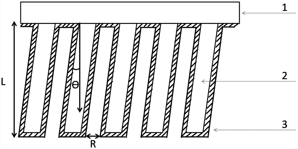
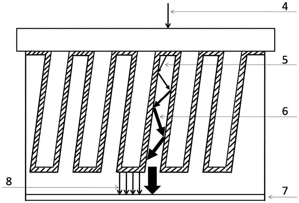
Micro-channel type incident window and production method thereof
A manufacturing method and a technology of an incident window, applied in the field of photoelectric detection, can solve problems such as complex structure, difficult preparation, and high cost of photodetectors, and achieve the effects of simple structure, easy preparation, and strong applicability
- Summary
- Abstract
- Description
- Claims
- Application Information
AI Technical Summary
Problems solved by technology
Method used
Image
Examples
Embodiment 1
[0053] A metal antimony cathode sensitive to X-rays is prepared by atomic layer deposition technology alone.
[0054] Step 1) ultrasonically clean the incident window in acetone, alcohol and deionized water for 10 minutes respectively;
[0055] Step 2) making a honeycomb structure on the incident window by using ordinary photolithography and ion beam etching or acid etching process;
[0056] Step 3) Perform high-temperature annealing on the entrance window etched into a honeycomb structure and then clean the entrance window again; (the cleaning process is the same as step 1)
[0057] Step 4) Put the above incident window into the atomic layer deposition system, and use the two precursor compounds of antimony to react to form a metal antimony film on the incident window at a temperature of 100 degrees. The thickness of the antimony film is displayed by a film thickness monitor , the general antimony film thickness is 6 nanometers to 40 nanometers.
Embodiment 2
[0059] A tellurium-cesium cathode sensitive to ultraviolet light is prepared by molecular beam epitaxy alone.
[0060] Step 1) The incident window was ultrasonically cleaned in acetone, alcohol and deionized water for 10 minutes each in sequence.
[0061] Step 2) making a honeycomb structure on the incident window by using ordinary photolithography and ion beam etching or acid etching process;
[0062] Step 3) Perform high-temperature annealing on the entrance window etched into a honeycomb structure and then clean the entrance window again; (the cleaning process is the same as step 1)
[0063] Step 4) Transfer the incident window to a vacuum system, grow a tellurium film on the incident window at room temperature, and observe the thickness of the tellurium film with a film thickness monitor, generally 20 nanometers in thickness;
[0064] Step 5) Raise the temperature of the vacuum chamber to 160 degrees, grow the cesium film, and observe the change of the photocurrent at the...
Embodiment 3
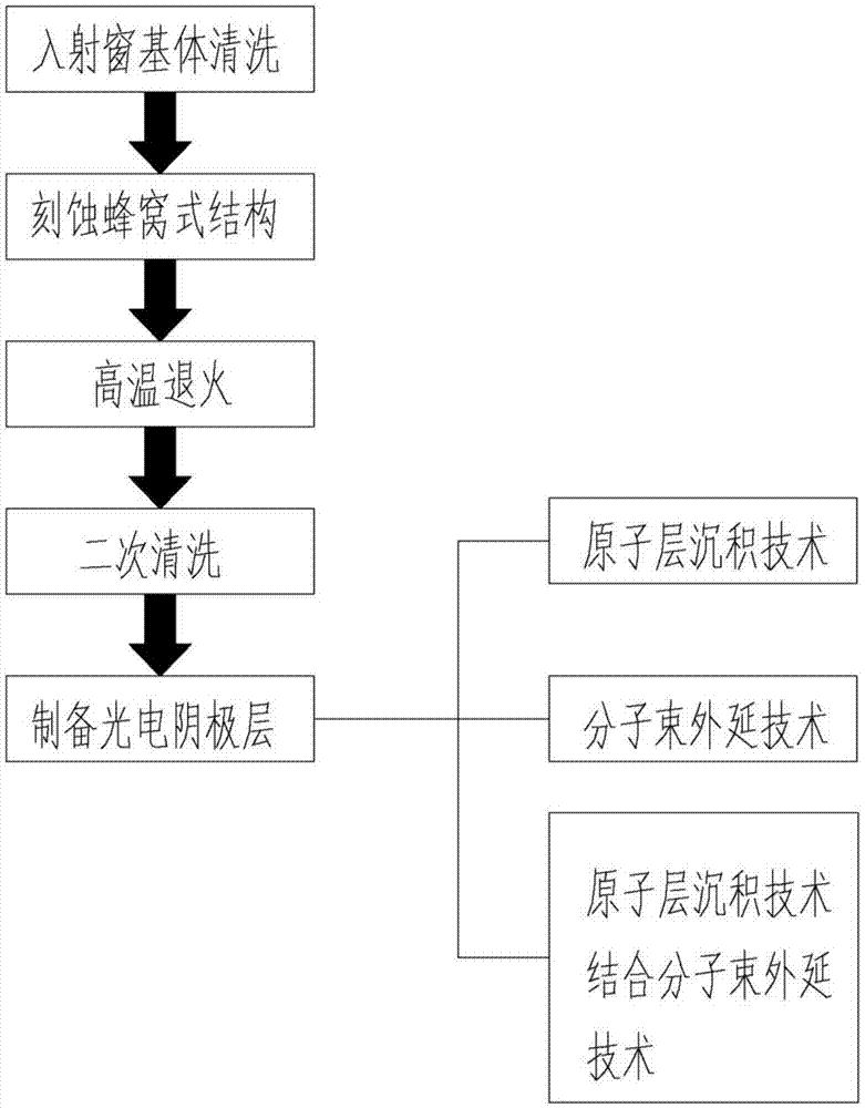
[0067] Such as image 3 Shown: Alkali metal photocathode is prepared by combining atomic layer deposition technology and molecular beam epitaxy technology.
[0068] Step 1) The incident window was ultrasonically cleaned in acetone, alcohol and deionized water for 10 minutes each in sequence.
[0069] Step 2) making a honeycomb structure on the incident window by using ordinary photolithography and ion beam etching or acid etching process;
[0070] Step 3) Perform high-temperature annealing on the entrance window etched into a honeycomb structure and then clean the entrance window again; (the cleaning process is the same as step 1)
[0071] Step 4) On the basis of the above-mentioned incident window substrate, a metal antimony (Sb) film is deposited on the surface of the substrate and the inner wall of the through hole by atomic layer deposition technology, and the thickness of the antimony film is about 8 nanometers. The atomic layer deposition technology can precisely contr...
PUM
 Abstract
Description
Claims
Application Information
 - R&D
- Intellectual Property
- Life Sciences
- Materials
- Tech Scout
- Unparalleled Data Quality
- Higher Quality Content
- 60% Fewer Hallucinations
Browse by: Latest US Patents, China's latest patents, Technical Efficacy Thesaurus, Application Domain, Technology Topic, Popular Technical Reports.
© 2025 PatSnap. All rights reserved.Legal|Privacy policy|Modern Slavery Act Transparency Statement|Sitemap|About US| Contact US: help@patsnap.com


