Fabricating method for graphene nanometer wall based on electromagnetic field reinforced plasma chemical vapor deposition
A graphene nanowall, chemical vapor deposition technology, applied in gaseous chemical plating, hybrid/electric double layer capacitor manufacturing, hybrid capacitor electrodes, etc., can solve the limited improvement of surface area, small effective surface area, and poor graphene wall structure. and other problems, to achieve the effect of improving specific capacitance and conductivity, increasing surface area, and improving dispersion.
- Summary
- Abstract
- Description
- Claims
- Application Information
AI Technical Summary
Problems solved by technology
Method used
Image

Examples
Embodiment 1
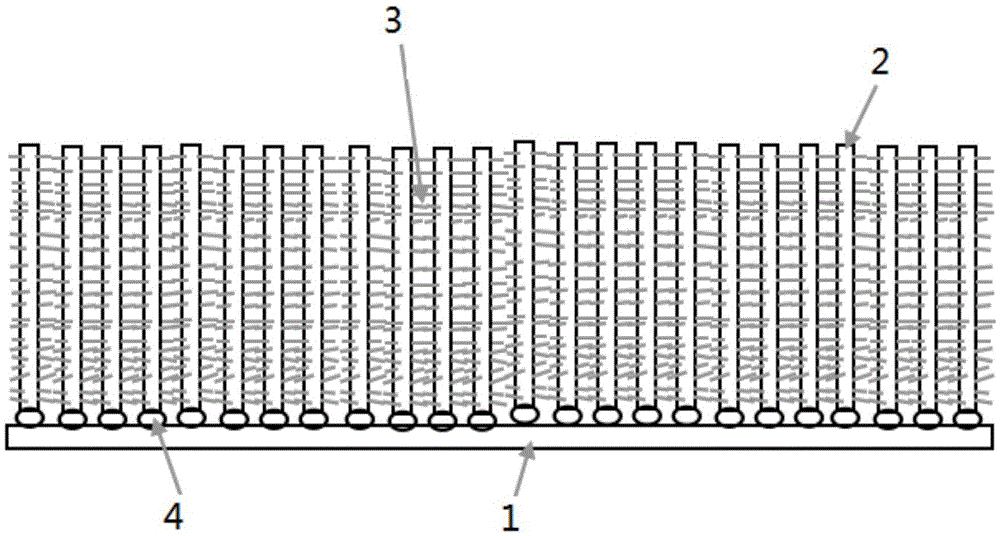
[0045] Using silicon wafers as substrates, PECVD is used to prepare graphene nanowalls, and 5nm gold nanofilms are grown on silicon wafers.
[0046] Step 1: grow one deck gold nano film on Si substrate by the mode of thermal evaporation, and its thickness is 5 nanometers.
[0047] Step 2: in step 1, the substrate of the gold nanofilm was deposited in the protective gas N 2 Heat treatment at 600-900 degrees Celsius for 2 hours; Figure 4 As shown, through the dewetting of the gold nano film, gold nanoparticles (clusters) are formed on the surface of the substrate, the size of which is 2-10 nanometers.
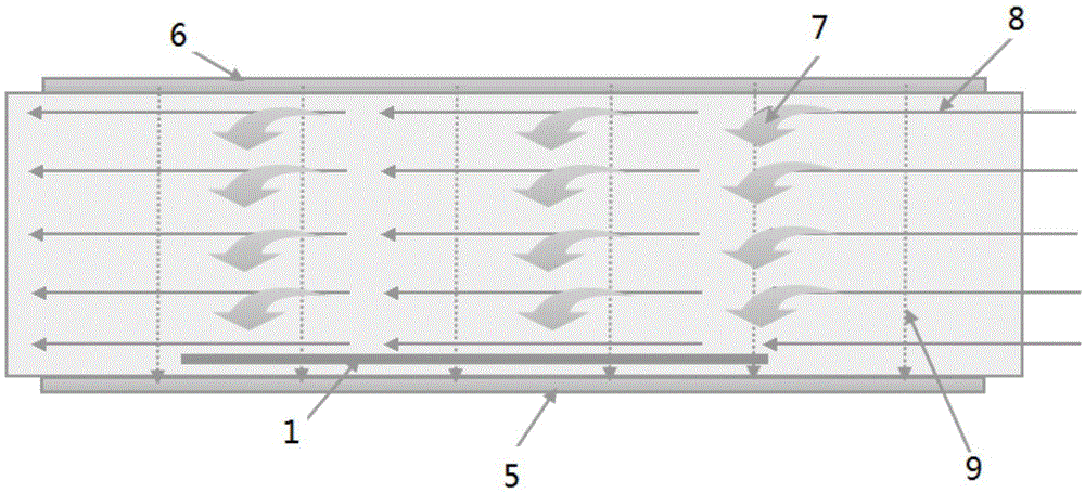
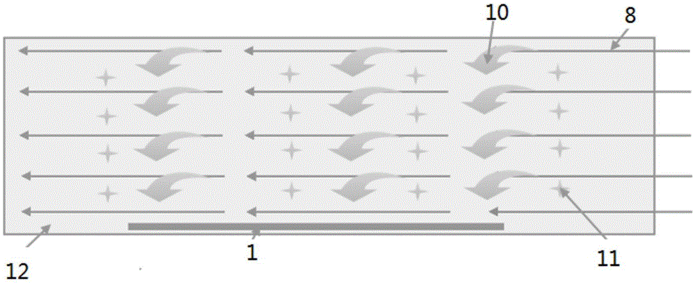
[0048] Step 3: Preparation of graphene nanowall: with CH 4 The plasma of the gas is used as a precursor, and the substrate obtained in step 2 is heated to 650-1000 degrees Celsius in a PECVD reactor; the graphene nano-wall is grown on the substrate by the PECVD method, and at the same time, as figure 2 As shown, a voltage U is applied in the vertical direction around the sub...
Embodiment 2
[0052] Using copper sheets as substrates, PECVD is used to prepare graphene nanowalls. A 10 nm gold nanofilm was grown on a silicon wafer.
[0053] Step 1: grow a layer of gold nano film on Si substrate by magnetron sputtering mode, its thickness is 10 nanometers.
[0054] Step 2: the substrate described in step 1 has deposited the gold nano film in protective gas (N 2 , Ar) heat treatment at 600-900 degrees Celsius for 2h. Such as Figure 4 As shown, through the dewetting of the gold nano film, gold nanoparticles (clusters) are formed on the surface of the substrate, the size of which is 5-15 nanometers.
[0055] Step 3: Preparation of graphene nanowall: with CH 4 Waiting for the plasma of carbon-containing gas as a precursor, heating the substrate obtained in step 2 to 650-1000 degrees Celsius in a PECVD reactor; growing graphene nanowalls on the substrate by PECVD;
[0056] While the graphene nanowalls are growing, such as figure 2 As shown, a voltage U is applied in...
Embodiment 3
[0061] Using silicon wafers as substrates, PECVD is used to prepare graphene nanowalls. A 20 nm gold nanofilm was grown on a silicon wafer.
[0062] Step 1: grow one deck gold nano film on Si substrate by the mode of ion sputtering, and its thickness is 20 nanometers.
[0063] Step 2: the substrate described in step 1 has deposited the gold nano film in protective gas (N 2 , Ar) heat treatment at 600-900 degrees Celsius for 2h. Such as Figure 4As shown, through the dewetting of the gold nano film, gold nanoparticles (clusters) are formed on the surface of the substrate, and the size is 10-20 nanometers.
[0064] Step 3: Preparation of graphene nanowall: with CH 4 The plasma of carbon-containing gas is used as a precursor, and the substrate obtained in step 2 is heated to 650-1000 degrees Celsius in a PECVD reactor. Grow graphene nanowalls on the substrate by PECVD method;
[0065] While the graphene nanowalls are growing, such as figure 2 As shown, a voltage U is appl...
PUM
| Property | Measurement | Unit |
|---|---|---|
| Thickness | aaaaa | aaaaa |
| Thickness | aaaaa | aaaaa |
| Thickness | aaaaa | aaaaa |
Abstract
Description
Claims
Application Information
 - R&D
- Intellectual Property
- Life Sciences
- Materials
- Tech Scout
- Unparalleled Data Quality
- Higher Quality Content
- 60% Fewer Hallucinations
Browse by: Latest US Patents, China's latest patents, Technical Efficacy Thesaurus, Application Domain, Technology Topic, Popular Technical Reports.
© 2025 PatSnap. All rights reserved.Legal|Privacy policy|Modern Slavery Act Transparency Statement|Sitemap|About US| Contact US: help@patsnap.com