High-voltage fast recovery diode chip employing gradient field limiting ring and production technology of high-voltage fast recovery diode chip

A recovery diode and production process technology, applied in the manufacturing of circuits, electrical components, semiconductor/solid-state devices, etc., can solve the problems of large difference in electric field distribution, large forward conduction voltage, and easy burnout of the pole tube chip, so as to achieve extended life, The effect of increasing the withstand voltage, enhancing the stability and reliability of the withstand voltage

Active Publication Date: 2016-04-13
桑德斯微电子器件(南京)有限公司
View PDF5 Cites 12 Cited by
  • Summary
  • Abstract
  • Description
  • Claims
  • Application Information

AI Technical Summary

Problems solved by technology

[0005] Aiming at the problems existing in the prior art that there are large differences in electric field distribution, low breakdown voltage, large leakage current, large forward conduction voltage, large power consumption, and easy burnout of the pole tube chip, the present invention provides

Method used


Image

  • High-voltage fast recovery diode chip employing gradient field limiting ring and production technology of high-voltage fast recovery diode chip
  • High-voltage fast recovery diode chip employing gradient field limiting ring and production technology of high-voltage fast recovery diode chip
  • High-voltage fast recovery diode chip employing gradient field limiting ring and production technology of high-voltage fast recovery diode chip

Examples


Embodiment 1

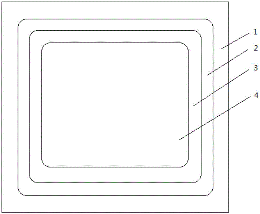
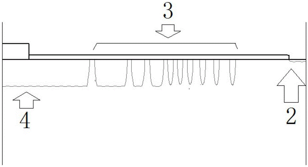
[0063] Such as figure 1 As shown, a high-voltage fast recovery diode chip with gradient electric field confinement ring includes a chip 1, an N+ cut-off ring 2, a gradient electric field confinement ring 3 and a P+ anode 4, and the chip 1 is a fast recovery diode chip; figure 2 As shown, the electric field confinement ring of gradient electric field confinement ring 3 has nine layers, and by design, the width of the electric field confinement ring is gradually reduced from 56 microns to 10 microns from the P+ anode to the N+ stop ring on the edge of the chip, and the distance between the electric field confinement rings is gradually changed. Larger, gradually increasing from 9 microns to 18 microns, the depth of the gradient electric field confinement ring 3 is the same as that of the P+ anode, and the depth is 40 microns. Such as Figure 4 As shown, the high-voltage potential linearly decreases from the P+ anode to the edge of the chip and the electric field is uniformly di...

Embodiment 2

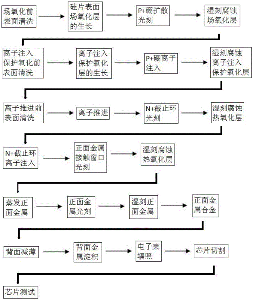
[0106] A production process of a high-voltage fast recovery diode chip with a gradient electric field confinement ring, the steps of which are as follows:

[0107] 1) Surface cleaning before field oxidation:

[0108] Configure a hydrofluoric acid solution, which is obtained by mixing a solution with a volume ratio of water:hydrofluoric acid=6:1, and the mass concentration of the hydrofluoric acid solution is 40%;

[0109] Configure No. 1 solution, which is obtained by mixing ammonia water: hydrogen peroxide solution: water = 1:1:5-1:2:7 in volume ratio, and the concentration of ammonia water is 27%;

[0110] Configure No. 2 solution, which is obtained by mixing the volume ratio of hydrogen chloride: hydrogen peroxide solution: water = 1:1:6-1:2:8. The mass concentration of hydrogen chloride is 37%, and the mass concentration of hydrogen peroxide solution is 30%. ;The cleaning sequence is as follows:

[0111] a. Soak the silicon wafer with hydrofluoric acid solution for 30s, ...

Embodiment 3

[0138] Embodiment 3 is basically the same as Embodiment 1, except that the backside thinning method in step 20) is wet etching.


PUM

PropertyMeasurementUnit
Depthaaaaaaaaaa
Breakdown voltageaaaaaaaaaa

Abstract

The invention discloses a high-voltage fast recovery diode chip employing a gradient field limiting ring and a production technology of the high-voltage fast recovery diode chip, and belongs to the field of semiconductor chips. The high-voltage fast recovery diode chip employing the gradient field limiting ring comprises a chip, an N+ cut-off ring, the gradient field limiting ring and a P+ anode, wherein the chip is the fast recovery diode chip; and a chip intercept layer sequentially comprises the chip, the N+ cut-off ring, the gradient field limiting ring and the P+ anode from right to left. The gradient field limiting ring comprises a plurality of field limiting rings of which the widths are gradually reduced from the P+ anode to the N+ cut-off ring; the widths of the field limiting rings are gradually reduced from the P+ anode to the edge of the chip; and the distances between the field limiting rings are gradually increased, so that the targets of linear reduction of a high voltage potential from the P+ anode to the edge of the chip and uniform field distribution are achieved; and the high-voltage fast recovery diode chip has the advantages of uniform field distribution, high breakdown voltage, low switching loss, low leakage current and low reverse power consumption.

Description

technical field [0001] The invention relates to the field of semiconductor chips, in particular to a gradient electric field confinement ring high voltage fast recovery diode chip and a production process thereof. Background technique [0002] Over the years, the turn-off characteristics of PN high-voltage power fast recovery diodes (FRDs) have attracted much attention. How to obtain a diode with short reverse recovery time, high softness and low reverse leakage current is the main goal of device design. In widely used high-speed hardware switching circuits, the softness of switching devices is of particular importance. However, in the conventional device design and manufacturing technology, improving the softness and increasing the switching speed are contradictory. The existing technology utilizes the absorption effect of vacancy defects induced by proton irradiation on platinum atoms to obtain local lifetime control, supplemented by the overall lifetime control technolo...

Claims


Application Information

Patent Timeline
IPC IPC(8): H01L29/06H01L21/329H01L29/868
CPCH01L29/0615H01L29/6609H01L29/868
Inventor 孙澜刘韵吉杨敏红单慧
Owner 桑德斯微电子器件(南京)有限公司
Why Eureka
Try Eureka