

Method for preparing silicon carbide super-junction structure through laser etching
A laser etching and silicon carbide technology, which is applied in semiconductor/solid-state device manufacturing, electrical components, circuits, etc., can solve the problems of high difficulty in groove shape adjustment, low SiC efficiency, poor groove uniformity, etc., and achieve groove The side wall is smooth, the uniformity is good, and the aspect ratio is improved
- Summary
- Abstract
- Description
- Claims
- Application Information
AI Technical Summary
Problems solved by technology
Method used
Image

Examples
Embodiment approach
[0034] According to one embodiment of the present invention, the method for preparing a silicon carbide superjunction structure includes:
[0035] S1, using laser etching to pattern the silicon carbide epitaxial wafer to form grooves on the surface of the silicon carbide epitaxial wafer;
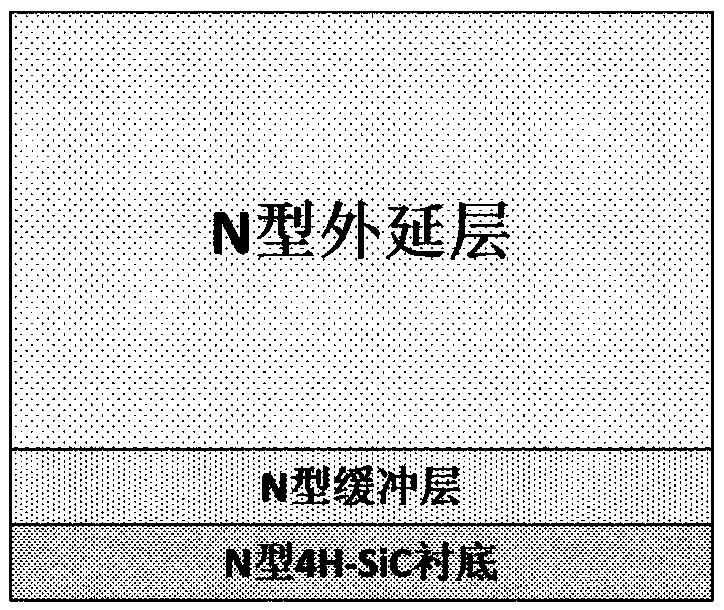
[0036] S2, growing silicon carbide epitaxially in the trench to form a silicon carbide superjunction structure, wherein the silicon carbide epitaxial wafer is one of an N-type epitaxial layer, a P-type epitaxial layer, and an N-type P-type mixed epitaxial layer. The impurity concentration range is 1×10 13 ~1×10 18 cm -3 , the doping type of the epitaxially grown silicon carbide is different from the doping type of the silicon carbide epitaxial wafer, the crystal form of the silicon carbide epitaxial wafer is 4H-SiC or 6H-SiC, the crystal form of the epitaxially grown silicon carbide is the same as that of the silicon carbide The epitaxial wafers have the same crystal form.
[0037] Accor...
Embodiment 1
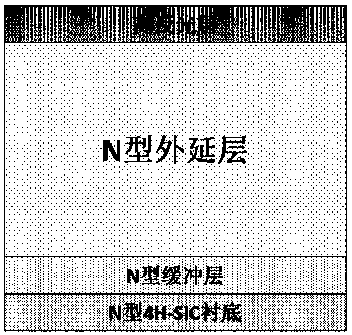
[0047] Deposit 5-10 groups of Si on 4H-SiC wafer with N-type epitaxial layer 3 N 4 / SiO 2 Laminated to form a highly reflective layer, the total thickness is 700nm ~ 2um, such as, image 3 shown.
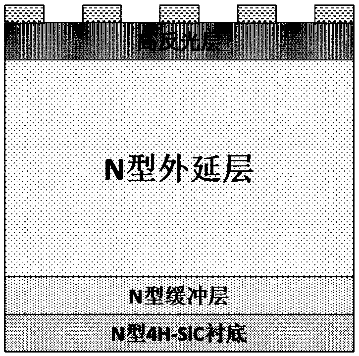
[0048] Through photolithography, the pattern required for laser etching is projected onto the photoresist on the surface of the SiC wafer to form a mask pattern, as shown in the attached Figure 4 shown.
[0049] Subsequently, under the mask of the photoresist, the highly reflective layer is etched by the ICP dry etching process. After the etching is completed, the photoresist is removed by the plasma stripping method, such as Figure 5 shown.
[0050] Subsequently, under the mask of the highly reflective layer, use a picosecond laser with a wavelength of 532nm and a pulse width of 10-800ps to etch SiC to the required depth, as Image 6 with 7 shown.
[0051] Subsequently, epitaxial growth is carried out in the SiC epitaxial furnace, and the P-type layer is uniformly grown t...
Embodiment 2
[0054] Deposit 5-10 groups of Si on 4H-SiC wafer with N-type epitaxial layer 3 N 4 / SiO 2 Laminated to form a highly reflective layer, the total thickness is 700nm ~ 2um, such as image 3 shown.
[0055] Through photolithography, the pattern required for laser etching is projected onto the photoresist on the surface of the SiC wafer to form a mask pattern, such as Figure 4 shown.
[0056] Subsequently, under the mask of the photoresist, the highly reflective layer is etched by the ICP dry etching process. After the etching is completed, the photoresist is removed by the plasma stripping method, such as Figure 5 shown.
[0057] Subsequently, under the mask of the highly reflective layer, use a picosecond laser with a wavelength of 532nm and a pulse width of 10-800ps to etch SiC to the required depth, as Image 6 with 7 shown
[0058] Subsequently, the Si on the SiC surface was removed by hydrofluoric acid buffer solution. 3 N 4 / SiO 2 Highly reflective layers such ...
PUM
| Property | Measurement | Unit |
|---|---|---|
| wavelength | aaaaa | aaaaa |
| wavelength | aaaaa | aaaaa |
| thickness | aaaaa | aaaaa |
Abstract
Description
Claims
Application Information