Diamond wire-cut polysilicon wafer with one-side texturing and texturing method thereof

A technology of diamond wire cutting and polycrystalline silicon wafers, which is applied in chemical instruments and methods, crystal growth, and final product manufacturing, can solve the problems of increasing battery processing costs and high cost of coating processes, and achieves reduction of silicon wafer processing steps and optimization of surface microscopic structure effect

Active Publication Date: 2017-08-04
LDK SOLAR XINYU HI TECH XINYU CO LTD
View PDF2 Cites 0 Cited by
  • Summary
  • Abstract
  • Description
  • Claims
  • Application Information

AI Technical Summary

Problems solved by technology

[0004] As a new silicon wafer product, diamond wire-cut polysilicon wafers currently have no mature texturing technology, and for the single-sided texturing of existing mortar-cut polysilicon wafers, most of the textured surfaces need to be protected by coating in advance ( Such as CN102181941A, CN104716224A), the cost of the coating process is relatively high, and subsequent processes need to be added to remove the coating protective layer on the suede surface, which increases the battery processing cost

Method used


Image

  • Diamond wire-cut polysilicon wafer with one-side texturing and texturing method thereof
  • Diamond wire-cut polysilicon wafer with one-side texturing and texturing method thereof
  • Diamond wire-cut polysilicon wafer with one-side texturing and texturing method thereof

Examples


Embodiment 1

[0086] A method for single-sided texturing of a diamond wire-cut polysilicon wafer, comprising the steps of:

[0087] (1) Cleaning pretreatment:

[0088] Prepare a potassium hydroxide solution with a mass fraction of 5%, heat it to 60°C, put the diamond wire-cut polysilicon wafer into the solution for alkaline cleaning for 6 minutes, and perform chemical etching and polishing to remove residual impurities and surface traces on the silicon wafer surface; then Rinse the silicon wafer in a pure water bath at 30°C for 5 minutes to remove residual lye on the surface of the silicon wafer;

[0089] Afterwards, place the silicon wafer in a hydrofluoric acid solution with a mass fraction of 6% for acid cleaning for 4 minutes to remove residual silicate substances on the surface of the silicon wafer, wherein the acid cleaning temperature is 35°C;

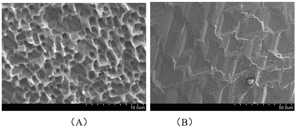
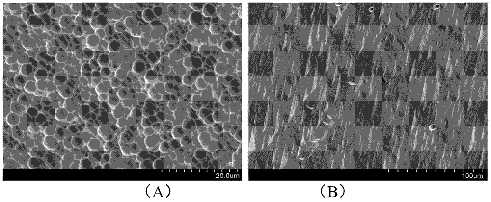
[0090] (2) Prepare a surface structure layer with micro-defects:

[0091] Insert the silicon wafers that have undergone the above cleaning...

Embodiment 2

[0103] A method for single-sided texturing of a diamond wire-cut polysilicon wafer, comprising the steps of:

[0104] (1) Cleaning pretreatment:

[0105] Prepare a potassium hydroxide solution with a mass fraction of 6%, heat it to 80°C, put the diamond wire-cut polysilicon wafer into the solution for alkaline cleaning for 3 minutes, and perform chemical etching and polishing to remove residual impurities and surface traces on the silicon wafer surface; then Rinse the silicon wafer in a pure water bath at 50°C for 3 minutes to remove residual lye on the surface of the silicon wafer;

[0106] Afterwards, place the silicon wafer in a hydrofluoric acid solution with a mass fraction of 8% for acid cleaning for 3 minutes to remove silicate substances remaining on the surface of the silicon wafer, wherein the acid cleaning temperature is 25°C;

[0107] (2) Prepare a surface structure layer with micro-defects:

[0108] Insert the silicon wafers that have undergone the above cleanin...

Embodiment 3

[0116] A method for single-sided texturing of a diamond wire-cut polysilicon wafer, comprising the steps of:

[0117] (1) Cleaning pretreatment:

[0118] Prepare a potassium hydroxide solution with a mass fraction of 10%, heat it to 70°C, put the diamond wire-cut polysilicon wafer into the solution for alkaline cleaning for 4 minutes, and perform chemical etching and polishing to remove residual impurities and surface traces on the silicon wafer surface; then Rinse the silicon wafer in a pure water bath at 40°C for 4 minutes to remove residual lye on the surface of the silicon wafer;

[0119] Afterwards, place the silicon wafer in a hydrofluoric acid solution with a mass fraction of 3% for acid cleaning for 3 minutes to remove residual silicate substances on the surface of the silicon wafer, wherein the acid cleaning temperature is 30°C;

[0120] (2) Prepare a surface structure layer with micro-defects:

[0121] Insert the silicon wafers that have undergone the above cleanin...


PUM

PropertyMeasurementUnit
heightaaaaaaaaaa
quality scoreaaaaaaaaaa

Abstract

The invention provides a single-surface texturing method for a diamond wire cut polycrystalline silicon wafer. The method comprises the following steps of taking diamond wire cut polycrystalline silicon wafers, inserting every two silicon wafers side by side in the same groove of a silicon wafer basket, putting the silicon wafer basket with the silicon wafers in a mixed solution containing hydrofluoric acid, hydrogen peroxide, silver nitrate and water and corroding the silicon wafer basket with the silicon wafers for 2-8 minutes, so as to prepare silicon wafers of a porous structure; sequentially putting the silicon wafers in an alkaline solution for alkali treatment, putting the silicon wafers in a nitric acid solution for acid treatment, and preparing a surface structural layer with slight defects on one surface of the silicon wafer; and texturing normally on the treated silicon wafers, water scrubbing and drying so as to obtain the polycrystalline silicon wafer with single surface textured. Through adoption of the method, the textured surface uniformly corroded can be formed on one surface of the diamond wire cut polycrystalline silicon wafer. The invention also provides the diamond wire cut polycrystalline silicon wafer with the single surface textured.

Description

technical field [0001] The invention belongs to the technical field of texturing of polycrystalline silicon wafers, and in particular relates to a diamond-wire-cut polycrystalline silicon wafer for single-side texturing and a texturing method thereof. Background technique [0002] Silicon wafers are widely used in photovoltaic solar energy, liquid crystal display and semiconductor fields. At present, the cutting of crystalline silicon wafers used in the photovoltaic industry mainly includes mortar multi-wire cutting technology and diamond wire cutting technology. In contrast, the latter uses diamond wires to polycrystalline silicon blocks. Multi-wire cutting to obtain polycrystalline silicon wafers has the characteristics of less surface damage, shallow and dense line marks, and low processing cost of silicon wafers, which has become the development direction of multi-wire cutting technology. [0003] In the production process of solar cells, texturing the surface of silicon...

Claims


Application Information

Patent Timeline
Patent Type & Authority Patents(China)
IPC IPC(8): H01L31/18C30B33/10H01L29/06
CPCC30B33/10H01L29/06H01L31/1804H01L31/182Y02P70/50
Inventor 付红平章金兵彭也庆
Owner LDK SOLAR XINYU HI TECH XINYU CO LTD
Why Eureka
Try Eureka