Copper-selective etching solution and titanium-selective etching solution

An etching solution and selective technology, applied in the field of semiconductor element processing, can solve the problems of low etching selectivity and uniformity

Inactive Publication Date: 2016-05-25
XITENG ELECTRONICS TECH SHANGHAI CO LTD
View PDF4 Cites 11 Cited by
  • Summary
  • Abstract
  • Description
  • Claims
  • Application Information

AI Technical Summary

Problems solved by technology

[0012] Aiming at the problem of relatively low etching selectivity and uniformity of the etchant used in the lead-free solder bump production group process in the prior art, the purpose of the present invention is to provide a method that can ensure the selectivity and uniformity of copper metal film etching. Uniform Copper Selective Etchant

Method used


Image

  • Copper-selective etching solution and titanium-selective etching solution
  • Copper-selective etching solution and titanium-selective etching solution
  • Copper-selective etching solution and titanium-selective etching solution

Examples


Embodiment 1~3 and comparative example 1~3

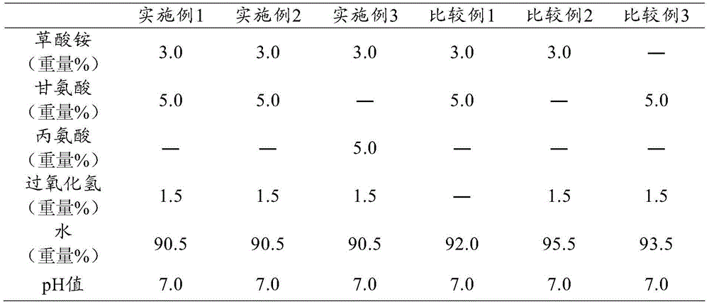
[0046] 1. The components and contents of Examples 1-3 and Comparative Examples 1-3 are shown in Table 1.

[0047] According to the components and proportions of Examples 1-3, the hydrogen peroxide is firstly diluted with water to obtain a copper oxidation solution, and then the remaining components and the remaining water are mixed to obtain a copper chelating solution. Finally, the copper oxide solution and the copper chelating solution are mixed to obtain a copper selective etching solution for etching. Then, according to the components and proportions of Comparative Examples 1-3, the copper contrast etching solution was prepared in the same way.

[0048] Among them, the pH value is adjusted by the copper etching solution pH regulator HCl, H 2 SO 4 , KOH and / or NaOH for adjustment.

[0049] The composition and content of table 1 copper selective etching solution, copper contrast etching solution

[0050]

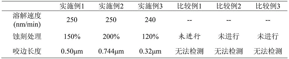
[0051] 2. Cu etching test

[0052] Etching speed test: place ...

Embodiment 4~8 and comparative example 4~7

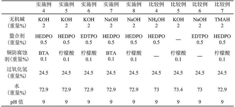
[0068] 1. The components and contents of Examples 4-8 and Comparative Examples 4-7 are shown in Table 4.

[0069] According to the components and proportions of Examples 4-8, first dilute the hydrogen peroxide with water to obtain a titanium oxide solution, then mix the rest of the components with the remaining water to obtain a titanium chelate solution, and finally use it in etching The oxidation solution and the chelating solution are mixed to obtain a titanium selective etching solution. According to the components and proportions of Comparative Examples 4-7, the same method was used to prepare a titanium contrast etching solution.

[0070] Wherein, the pH value is adjusted by boric acid, hydrochloric acid, sulfuric acid and / or phosphoric acid as a pH regulator of the titanium etching solution.

[0071] The composition and content of table 4 titanium selective etching solution, titanium contrast etching solution

[0072]

[0073] HEDPO: 1-Hydroxyethane-1,1'-diphosphat...

Embodiment 9 and comparative example 8

[0094] 1. Fabrication of semiconductor substrates

[0095] First, a thermal oxide film (SiO2) with a thickness of 10nm 2 ) on a 6 cm Si substrate by sputtering to deposit a 100nm thick Ti layer, and then on this Ti / SiO 2 On the / Si substrate, a 100nm-thick Cu stacked layer continues to be deposited. And in these Cu / Ti / SiO 2 The / Si substrate is covered with a positive film photoresistive resin coating (film thickness about 60 μm), and the model is formed by photolithography technology. After that, a Cu layer (Cu column) with a height (Cu column film thickness) of about 40 μm and a lateral width (Cu column width) of about 60 μm was deposited by electroplating, and then covered with Ni layer and Sn / Ag (96.5 :3.5) Alloy laminate (thickness about 15μm, width about 60μm). Finally, the photosensitive resistor resin coating is removed to obtain a semiconductor substrate.

[0096] The semiconductor substrate was cut into small pieces with a length of 1 cm x a width of 1 cm and us...


PUM

PropertyMeasurementUnit
thicknessaaaaaaaaaa
thicknessaaaaaaaaaa
thicknessaaaaaaaaaa

Abstract

The invention discloses a copper-selective etching solution prepared from a copper oxidizing solution and a copper chelating solution. The copper oxidizing solution is prepared from an oxidizing agent and/or water, the copper chelating solution is prepared from oxalate, amino carboxylic acid and water, and the pH value of the copper-selective etching solution is 6.0-8.5; the copper-selective etching solution can selectively and uniformly etch copper. The invention further discloses a titanium-selective etching solution prepared from a titanium oxidizing solution and a titanium chelating solution. The titanium oxidizing solution is prepared from hydrogen peroxide and/or water, the titanium chelating solution is prepared from a phosphorous acid chelating agent, a copper anticorrosive agent, inorganic base and water, and the pH value of the titanium-selective etching solution is 7-10; the titanium-selective etching solution can selectively and uniformly etch titanium. In the manufacturing process of lead-free solder bumps, lead-free solder bumps with the good size reproducibility can be conveniently and quickly manufactured on a semiconductor substrate by using the copper-selective etching solution and the titanium-selective etching solution for etching.

Description

technical field [0001] The invention belongs to the technical field of semiconductor element processing, and in particular relates to a copper selective etching solution and a titanium selective etching solution. Background technique [0002] The ROHS (Restriction of Hazardous Substences) international standard makes mandatory regulations on the management of lead (Pb)-free semiconductor components (such as bumps) that are widely used in semiconductors, printed circuit boards, IC cards and other equipment. The process of making lead-free solder bumps is as follows: firstly, on a semiconductor substrate (such as a silicon (Si) substrate), a barrier layer of titanium (Ti) with a thickness of several hundred nanometers and a layer of titanium (Ti) metal film with a thickness of several hundred nanometers are sequentially deposited on a semiconductor substrate (such as a silicon (Si) substrate). Electroplating copper seed layer or copper (Cu) metal film of the electrode; secondl...

Claims


Application Information

Patent Timeline
Patent Type & Authority Applications(China)
IPC IPC(8): C23F1/14C23F1/38
CPCC23F1/14C23F1/38
Inventor 江月华
Owner XITENG ELECTRONICS TECH SHANGHAI CO LTD
Why Eureka
Try Eureka