

High-density semiconductive single-walled carbon nanotube horizontal array and preparation method thereof
A single-walled carbon nanotube, semiconductor technology, applied in the field of high-density semiconducting single-walled carbon nanotube horizontal array and its preparation, can solve the problem of inability to obtain high-density semiconducting single-walled carbon nanotube horizontal array, density drop, etc. problems, to achieve the effect of low cost, good repeatability and broad application prospects
- Summary
- Abstract
- Description
- Claims
- Application Information
AI Technical Summary
Problems solved by technology
Method used
Image

Examples
Embodiment 1
[0044] 1) Use a pipette gun to pipette 34 μL of tetrabutyl phthalate and 61 μL of ethanolamine and dissolve them in 150 mL of absolute ethanol solution, stir well, and dissolve the mixed solution of ethanol and ultrapure water (50 mL of ethanol, 9 μL of ultrapure water) Add dropwise to the above mixed solution, and continue to stir to obtain a transparent sol with a titanium element concentration of 0.5 mmol / L.
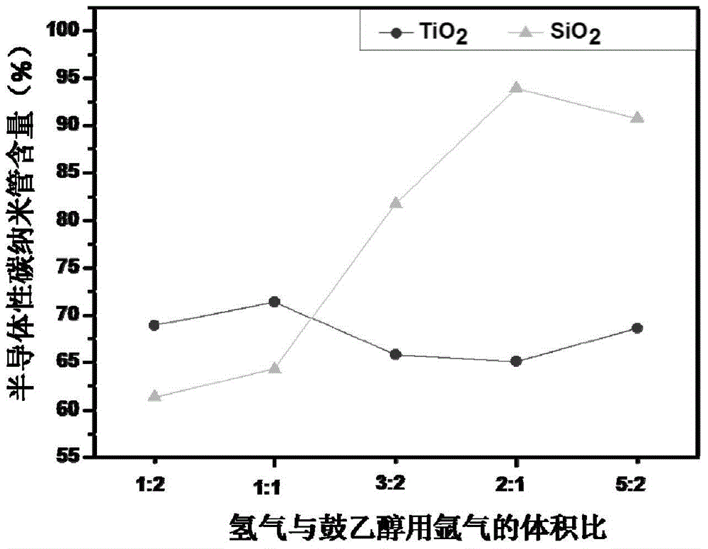
[0045] 2) Dip a small amount of the above TiO 2 Sol, using the microcontact printing method to prepare linear patterned catalyst strips on the ST-cut quartz single crystal substrate, and the direction of the strips is perpendicular to the lattice direction of the substrate surface. Put the catalyst-loaded substrate into a chemical vapor deposition system, raise the temperature to 800°C, and calcinate in air for 20 minutes to obtain TiO 2 For nanoparticles, 300 sccm argon gas was introduced for 5 minutes to exhaust the air in the system, and then ethanol was bubbled w...
Embodiment 2
[0047] 1) Prepare titania sol according to the method of Example 1, spin-coat it on the α-alumina surface a, place the substrate spin-coated with the catalyst in a muffle furnace, anneal in air at 1100°C for 8h, then cool down to 300°C for 10h , and then cooled naturally to room temperature.
[0048] 2) Put the above catalyst-loaded and annealed alumina substrate into a chemical vapor deposition system, raise the temperature to 850°C, calcine in air for 20 minutes, pass 300 sccm argon gas into it for 5 minutes, then bubble ethanol with 150 sccm argon gas, and pass through 300sccm hydrogen gas, grown at a growth temperature of 850° C. for 30 minutes to prepare a horizontal array of high-density semiconducting single-walled carbon nanotubes.
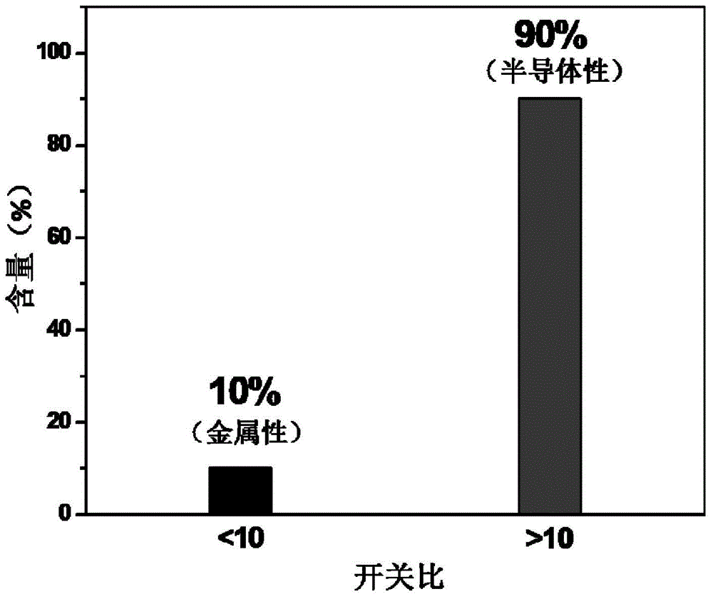
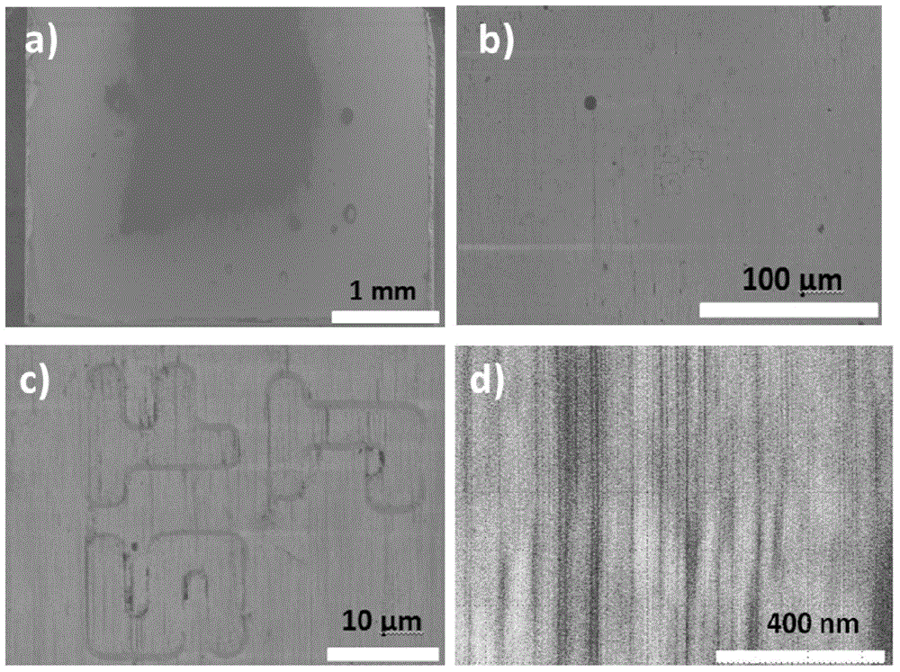
[0049] High-resolution scanning electron microscopy (SEM) and atomic force microscopy (AFM) characterize its density to 60-80 roots / micron, such as image 3 , Figure 4 shown. Its Raman spectrum is as Figure 5 a and 5b( Figure 5 a s...
PUM
 Abstract
Description
Claims
Application Information