

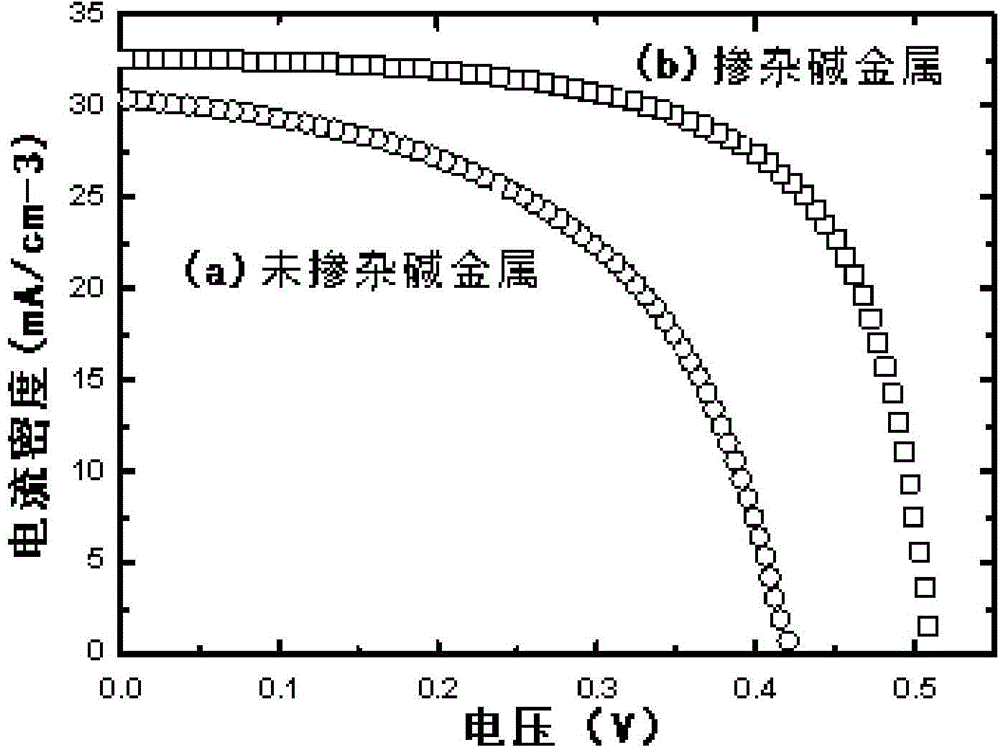
Alkali metal doping method for preparing CIGS absorbing layer on flexible substrate
A flexible substrate and absorption layer technology, which is applied in the field of alkali metal doping of CIGS absorption layers prepared on flexible substrates, can solve the problem of difficulty in applying large-area CIGS deposition and large-scale production, affecting the growth process of CIGS thin films, and the crystallization quality of CIGS thin films. Reduce problems such as reducing, and achieve the effect of being beneficial to large-scale production, improving photoelectric conversion efficiency, and improving P-type conductivity characteristics
- Summary
- Abstract
- Description
- Claims
- Application Information
AI Technical Summary
Problems solved by technology
Method used
Image

Examples
Embodiment 1
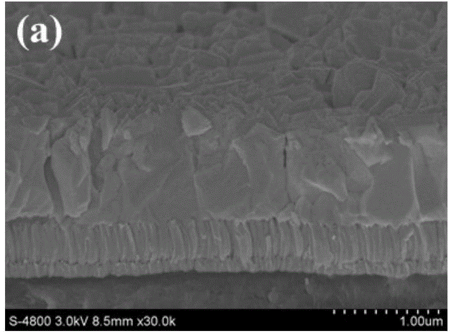
[0031] An alkali metal doping method for preparing a CIGS absorbing layer on a flexible substrate, using a low-temperature co-evaporation process to deposit a small-area CIGS absorbing layer, and preparing a flexible CIGS thin film solar cell. Using polyimide with a thickness of 50 μm as the substrate, a thin layer of Mo with a thickness of 0.5 μm to 1 μm was first deposited on the substrate by DC magnetron sputtering process as the positive electrode of the battery, and a CIGS thin film was deposited on it. During the deposition process, the vacuum pressure of the chamber was kept at 1×10 -3 Pa or so. The first step is to co-evaporate In, Ga and Se elements at a substrate temperature of 300°C-350°C to form (In 0.7 Ga 0.3 ) 2 Se 3 For the preset layer, the temperature of the evaporation source of Ga and In is kept constant at 900°C-1000°C and 800°C-900°C respectively, the evaporation source of Se is kept constant in the range of 220°C-280°C, the evaporation time is 20min, ...
Embodiment 2
[0034] See attached image 3 with Figure 4 .
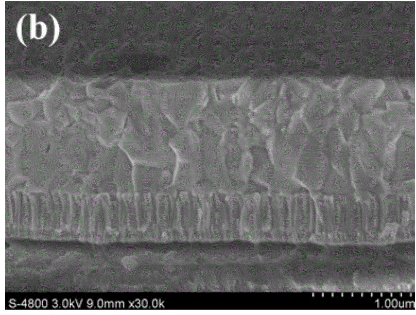
[0035] A method for preparing CIGS absorbing layer alkali metal doping on a flexible substrate, using a metal (such as stainless steel, titanium, etc.) foil with a thickness of 50 μm as a substrate to prepare a flexible CIGS absorbing layer and a solar cell, the cell structure is the same as in Example 1. Using the same evaporation process parameters and alkali metal doping method as in Example 1, a stainless steel substrate CIGS thin film solar cell was obtained.
[0036] attached image 3 with Figure 4 The medium vacuum evaporation chamber is made of #316 stainless steel plate through seamless welding process; the water cooling pipeline is seamlessly welded on the surface of the vacuum chamber, and the temperature of the cold water flowing in is about 10°C. The right side of the vacuum chamber is equipped with a vacuum pumping system 4, and the left side is equipped with an ionization gauge 5 for testing the pressure of th...
Embodiment 3
[0039] See attached Figure 5 .
[0040] An alkali metal doping method for preparing a CIGS absorbing layer on a flexible substrate, using a roll-to-roll co-evaporation process to deposit a large-area CIGS absorbing layer, and preparing a flexible CIGS thin film solar cell. Using polyimide with a thickness of 50 μm as the substrate, a 0.5 μm-0.8 μm thick Mo back electrode was first deposited on the substrate by a DC magnetron sputtering process, and a CIGS thin film was deposited on it by roll-to-roll evaporation. Figure 5 The roll-to-roll evaporator shown. The device is in the shape of a rectangular parallelepiped as a whole, and is made of #316 stainless steel plate through seamless welding process; the water-cooling pipeline is seamlessly welded on the surface of the vacuum chamber, and the temperature of the cold water flowing in is about 10°C. The device includes a first chamber 17 and a second chamber 18 , a vacuum valve 24 and a vacuum system 25 . The first chamber ...
PUM
| Property | Measurement | Unit |
|---|---|---|
| Carrier concentration | aaaaa | aaaaa |
| Thickness | aaaaa | aaaaa |
| Thickness | aaaaa | aaaaa |
Abstract
Description
Claims
Application Information