Tunnel silicon oxide passivated contact solar cell and preparation method thereof

A technology for tunneling through a silicon-oxygen-nitride layer and a solar cell is applied in the field of solar cells, which can solve the problems of destroying the integrity of the silicon oxide layer, weakening the field passivation effect of the silicon wafer, affecting the filling factor, etc., so as to reduce the occurrence of leakage current and reduce the leakage current. Recombination speed, good chemical passivation effect, effect of reducing interface state density

Active Publication Date: 2016-07-06
NINGBO INST OF MATERIALS TECH & ENG CHINESE ACADEMY OF SCI
View PDF5 Cites 22 Cited by
  • Summary
  • Abstract
  • Description
  • Claims
  • Application Information

AI Technical Summary

Problems solved by technology

However, the silicon oxide layer also has disadvantages as a passivation tunneling layer. Due to the large forbidden band width of silicon oxide (about 8.9eV), the electron and hole transport barrier is relatively large, which is not conducive to the transmission of electrons or holes. Transport, when the thickness of the silicon oxide layer used as a tunneling oxide exceeds 2nm, its tunneling efficiency begins to drop significantly, which affects the fill factor. In order to enable electrons to tunnel through the silicon oxide layer as a passivation tunneling layer, it is necessary to The silicon layer is made very thin, usually controlled below 2nm, so holes are easy to form during the preparation process, resulting in increased leakage current, and in the subsequent high-temperature annealing process, atoms such as phosphorus in the doped thin-film silicon layer are easy to diffuse into as In the silicon oxide layer of the passivation tunneling layer, the integrity of the silicon oxide layer as the passivation tunneling layer is destroyed, resulting in increased leakage current and recombination; in addition, the thin silicon oxide layer has a low defect energy level density, with Positive charge density is low, and the field passivation effect on silicon wafers is weakened

Method used


Image

  • Tunnel silicon oxide passivated contact solar cell and preparation method thereof
  • Tunnel silicon oxide passivated contact solar cell and preparation method thereof
  • Tunnel silicon oxide passivated contact solar cell and preparation method thereof

Examples


preparation example Construction

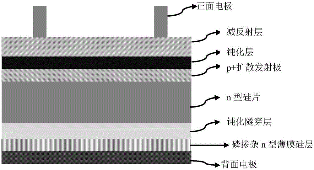
[0041] The invention provides a method for preparing a tunneling silicon oxygen nitride layer passivation contact solar cell, the solar cell includes a silicon wafer, a passivation tunneling layer, a doped thin film silicon layer, and the passivation tunneling layer Located between the silicon wafer and the doped thin-film silicon layer, wherein the preparation method includes the following steps: pretreating the silicon wafer, and forming a silicon oxide layer on one side or both sides of the pretreated silicon wafer Then generate a silicon oxynitride layer or a silicon nitride layer on the surface of the silicon oxide layer, and then anneal the obtained product; or generate a silicon oxynitride layer on one side or both sides of the pretreated silicon wafer , and then a silicon nitride layer is formed on the surface of the silicon oxynitride, and then the obtained product is annealed; or a silicon oxide layer is formed on one side or both sides of the pretreated silicon wafer...

Embodiment 1

[0075] In this embodiment, the n-type silicon wafer is used as the substrate. First, the n-type silicon wafer is pretreated. Carry out cleaning velvet, so that remove mechanical damage layer, greasy dirt and metal impurity, form undulating velvet surface simultaneously on the surface; On the n-type silicon wafer side after pretreatment, grow a layer thickness by 68% concentrated nitric acid 1.5nm silicon oxide (SiO x ) layer; then the n-type silicon wafer that generates the silicon oxide layer is placed in a plasma-enhanced chemical vapor deposition (PECVD) device, in the reaction gas SiH 4 The flow rate is 1sccm, NH 3 The flow rate is 10sccm, the cavity pressure is 10Pa, the temperature is 100°C, and the RF power is 50W, the reaction is 0.5min; after that, it is annealed at 800°C for 60min in a nitrogen-hydrogen mixed (FormingGas) atmosphere to eliminate defects and generate silicon oxide / Gradient silicon oxynitride stack; by plasma-enhanced chemical vapor deposition, the ...

Embodiment 2

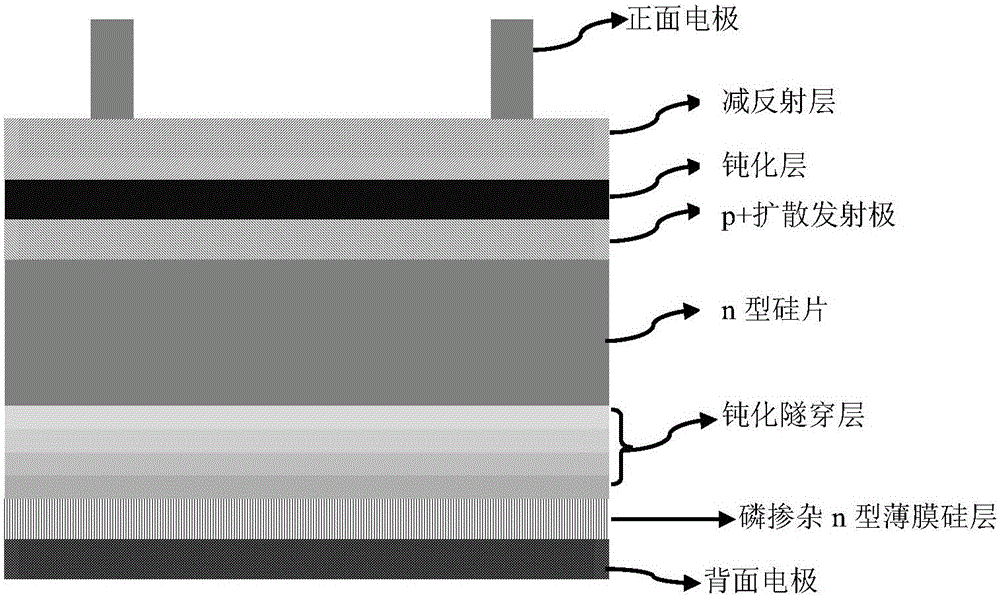
[0078] Solar cells are prepared in the same manner as in Example 1, except that silicon oxide (SiO x ) layer; then the n-type silicon wafer that generates the silicon oxide layer is placed in a plasma-enhanced chemical vapor deposition (PECVD) device, in the reaction gas SiH 4 The flow rate is 1sccm, NH 3 The flow rate is 10sccm, the cavity pressure is 10Pa, the temperature is 100°C, and the radio frequency power is 50W, the reaction is 0.5min; then annealing is carried out at 850°C for 30min in a nitrogen-hydrogen mixed (FormingGas) atmosphere, and the solar cell A2 is obtained.

[0079] The surface saturation current density, open circuit voltage, short circuit current, fill factor, and conversion efficiency of solar cell A2 were measured in the same manner as in Example 1. The results of the passivation tunneling layer thickness and composition of solar cell A2 are shown in Table 1.


PUM


Abstract

The invention provides a solar cell. The solar cell comprises a silicon wafer, a passivated tunnel layer and a doping thin film silicon layer, wherein passivated tunnel layer is arranged between the silicon wafer and the doping thin film silicon layer, the passivated tunnel layer is one of a silicon oxide/silicon oxynitride gradient lamination layer, a silicon oxynitride/silicon nitride gradient lamination layer and a silicon oxide/silicon oxynitride/silicon nitride gradient lamination layer, the silicon oxynitride is nitrogen doping silicon oxide or oxygen doping silicon nitride, and the nitrogen concentration of the silicon oxide/silicon oxynitride gradient lamination layer, the silicon oxynitride/silicon nitride gradient lamination layer and the silicon oxide/silicon oxynitride/silicon nitride gradient lamination layer is gradiently reduced from a part far away from a silicon wafer side to the silicon wafer side. Since the tunnel barriers of silicon nitride and silicon oxynitride are relatively low, the thickness of the passivated tunnel layer can be appropriately widened on the premise of ensuring the tunnel efficiency, thus, the holes of the passivated tunnel layer are favorably reduced, the generation and combination rate of current leakage are reduced, the process window is expanded, and the process stability is improved.

Description

technical field [0001] The invention relates to the field of solar cells, in particular to a tunneling silicon-oxygen-nitride layer passivation contact solar cell and a preparation method thereof. Background technique [0002] Tunnel oxide passivated contact (TunnelOxidePassivatedContact, TOPCon) solar cell is a new type of silicon solar cell proposed by Fraunhofer Institute for Solar Energy Research in Germany in recent years. The battery uses an n-type silicon wafer, and the back of the silicon wafer is covered with a layer of silicon oxide layer below 2nm as a passivation tunneling layer, and then covered with a layer of doped thin-film silicon layer to passivate the back of the battery. The basic cell structure of the tunnel oxide passivation contact solar cell see figure 1 As shown, the back structure of the solar cell is an n-type silicon wafer, a passivation tunneling layer (silicon oxide layer), a doped n-type thin film silicon layer, and a metal electrode layer. W...

Claims


Application Information

Patent Timeline
Patent Type & Authority Applications(China)
IPC IPC(8): H01L31/048H01L31/0216
CPCY02E10/50H01L31/048H01L31/0216H01L31/02167H01L31/0481
Inventor 叶继春曾俞衡高平奇韩灿廖明墩王丹蔡亮
Owner NINGBO INST OF MATERIALS TECH & ENG CHINESE ACADEMY OF SCI
Why Eureka
Try Eureka