Preparation method of p type copper oxide thin film with low resistivity and high carrier concentration
A high-carrier, low-resistivity technology, applied in the direction of ion implantation plating, metal material coating process, coating, etc., can solve the problems that affect the performance of copper oxide electronic and optoelectronic devices, low carrier concentration, and resistivity. Advanced problems, achieve the effect of low resistivity, high carrier concentration and simple operation
- Summary
- Abstract
- Description
- Claims
- Application Information
AI Technical Summary
Problems solved by technology
Method used
Image
Examples
Embodiment 1
[0013] Ordinary glass substrates were ultrasonically cleaned in acetone, ethanol, and deionized water for 5 minutes in sequence, and dried with nitrogen. Weigh 0.98g of copper oxide powder and 0.02g of metallic lithium powder, place them in a metal mold with a diameter of 2cm, and press the target with a tablet press at a pressure of 10MPa to obtain a copper oxide target doped with 1wt% lithium. The cleaned ordinary glass substrate and the copper oxide target doped with 2wt% lithium were transported to the deposition chamber of the laser pulse deposition equipment by a robot, and the deposition chamber was evacuated to 1×10 by mechanical pump and molecular pump. -4 Pa, adjust the distance between the glass substrate and the copper oxide target to be 6cm, then heat the glass substrate to 500°C, then open the oxygen vent valve, feed oxygen into the deposition chamber, and turn on the mass flow meter to control the oxygen flow to 18sccm, Adjust the pressure of the deposition cham...
Embodiment 2
[0017] In Example 1, the copper oxide target doped with 2 wt % lithium was replaced by the copper oxide target doped with 1 wt % lithium, and other steps were the same as in Example 1 to obtain a p-type copper oxide film.
Embodiment 3
[0019] In Example 1, the copper oxide target doped with 4 wt % lithium was used to replace the copper oxide target doped with 2 wt % lithium, and other steps were the same as in Example 1 to obtain a p-type copper oxide film.
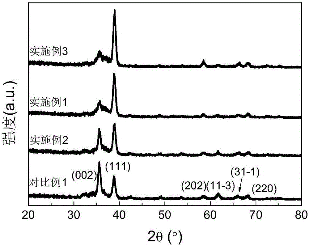
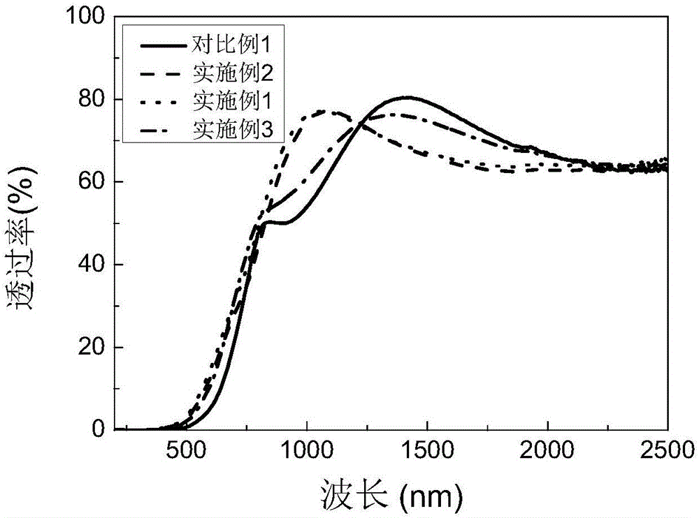
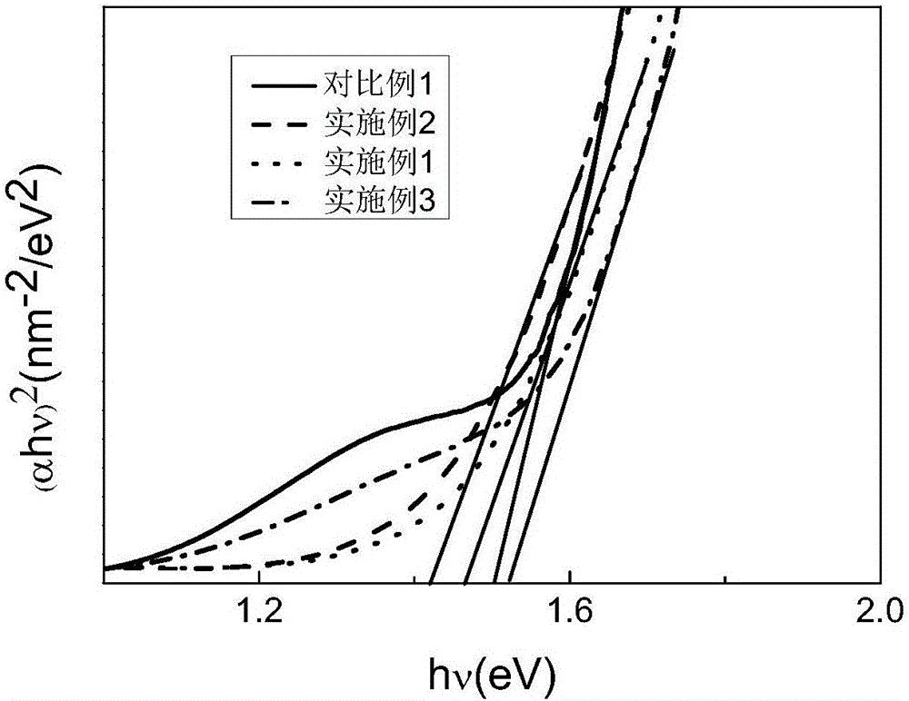
[0020] The inventor used X-ray diffractometer, ultraviolet-visible-near-infrared spectrometer, and Hall effect tester to characterize the p-type copper oxide thin films prepared in Examples 1 to 3 and Comparative Example 1. The results are shown in Figure 1~3 and Table 1.
[0021] Table 1 The electrical properties of the p-type copper oxide film prepared in Examples 1 to 3 and Comparative Example 1
[0022]
[0023] Depend on figure 1 It can be seen that the p-type copper oxide films prepared in Examples 1-3 and Comparative Example 1 all have diffraction peaks of CuO (002) and (111) crystal planes, but compared with the p-type copper oxide films prepared in Comparative Example 1 without lithium Copper thin film, the diffraction peak of the p-type ...
PUM
| Property | Measurement | Unit |
|---|---|---|
| Optical bandgap | aaaaa | aaaaa |
Abstract
Description
Claims
Application Information


