Fabrication method of wafer-level uniaxial strain geoi based on silicon nitride stress film and scale effect

A technology of uniaxial strain and scale effect, applied in the field of microelectronics, can solve the problems of wafer fragmentation, poor reliability, and small strain, and achieve the effects of increased strain, low cost, and large strain

Active Publication Date: 2018-09-11
XIDIAN UNIV
View PDF3 Cites 0 Cited by
  • Summary
  • Abstract
  • Description
  • Claims
  • Application Information

AI Technical Summary

Problems solved by technology

[0012] However, this method has the following disadvantages: 1) Poor compatibility with traditional integrated circuit technology: In order to obtain GeOI with different strains, this method needs to make additional bending tables with different curvature radii, and the manufactured bending tables need to be compatible with existing With annealing equipment
2) Poor reliability: This process requires the use of pressure rods to apply mechanical force to bend the GeOI wafer, which will introduce defects into the top layer of Ge; if the GeOI wafer bends too much, it will cause wafer fragmentation
3) Due to the fear of breaking the GeOI wafer, the bending degree of the mechanical bending cannot be too large, which limits the amount of strain introduced in the top layer Ge, and the amount of strain that can be achieved is small

Method used


Image

  • Fabrication method of wafer-level uniaxial strain geoi based on silicon nitride stress film and scale effect
  • Fabrication method of wafer-level uniaxial strain geoi based on silicon nitride stress film and scale effect
  • Fabrication method of wafer-level uniaxial strain geoi based on silicon nitride stress film and scale effect

Examples


Embodiment 1

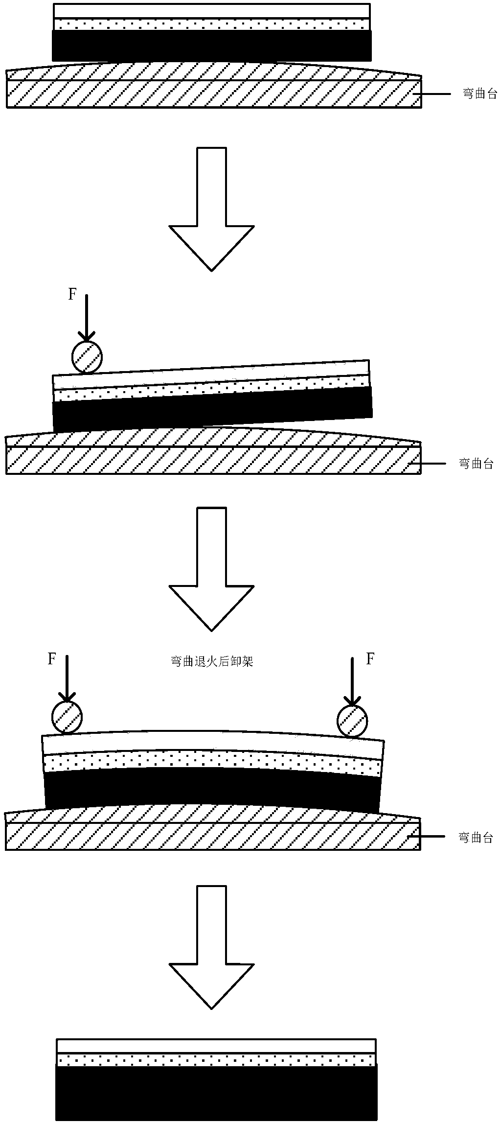
[0037] Example 1, preparing a 3-inch uniaxially strained GeOI wafer material.

[0038] Step 1: Clean the GeOI wafer to remove surface contamination.

[0039] (1.1) Use acetone and isopropanol to alternately perform ultrasonic cleaning on the GeOI wafer to remove organic contamination on the substrate surface;

[0040] (1.2) Prepare a 1:1:3 mixed solution of ammonia, hydrogen peroxide, and deionized water, and heat it to 120°C. Place the GeOI wafer in the mixed solution for 12 minutes, take it out and rinse it with a large amount of deionized water. To remove inorganic pollutants on the surface of GeOI wafers;

[0041] (1.3) Soak the GeOI wafer in HF acid buffer for 2 minutes to remove the oxide layer on the surface.

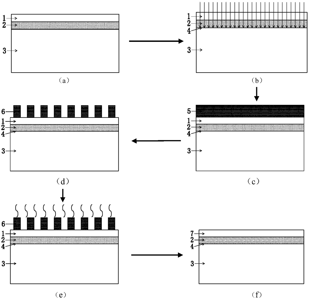
[0042] Step 2: Ion implantation.

[0043] Perform ion implantation on the cleaned GeOI wafer to make Si substrate 3 and SiO 2 The interface 4 of the buried insulating layer 2 is loose, such as figure 2 as shown in b.

[0044] The process conditions of ion im...

Embodiment 2

[0056] Example 2, preparing a 6-inch uniaxial compressively strained GeOI wafer material.

[0057] Step 1: Cleaning the GeOI wafer to remove surface contamination.

[0058] The implementation of this step is the same as step 1 of Embodiment 1.

[0059] Step 2: Implant the cleaned GeOI wafer with a dose of 1.3E15cm -2 , He ions with energy 130Kev to make Si substrate 3 and SiO 2 The interface 4 of the buried insulating layer 2 is loose, such as figure 2 as shown in b.

[0060] Step 3: Using the PECVD plasma enhanced chemical vapor deposition process, deposit a tensile stress SiN thin film 5 with a thickness of 1.0 μm and a stress of 1.1 GPa on the surface of the top layer Ge layer 1 of the ion-implanted GeOI wafer, such as figure 2 as shown in c.

[0061] The deposition process conditions are: high-frequency HF power is 1.3KW, low-frequency LF power is 0.2KW, high-purity SiH 4 The flow rate is 0.3slm, high-purity NH 3 The flow rate is 1.8 slm, the flow rate of high-pur...

Embodiment 3

[0069] Example 3, preparing a 12-inch uniaxially strained GeOI wafer material.

[0070] Step A: Cleaning the GeOI wafer to remove surface contamination.

[0071] The implementation of this step is the same as step 1 of Embodiment 1.

[0072] Step B: Perform ion implantation on the cleaned GeOI wafer to make Si substrate 3 and SiO 2 The interface 4 of the buried insulating layer 2 is loose, such as figure 2 as shown in b.

[0073] The ion implantation process is: the implanted ions are He ions, and the implantation dose is 1.3E16cm -2 , inject energy 170Kev.

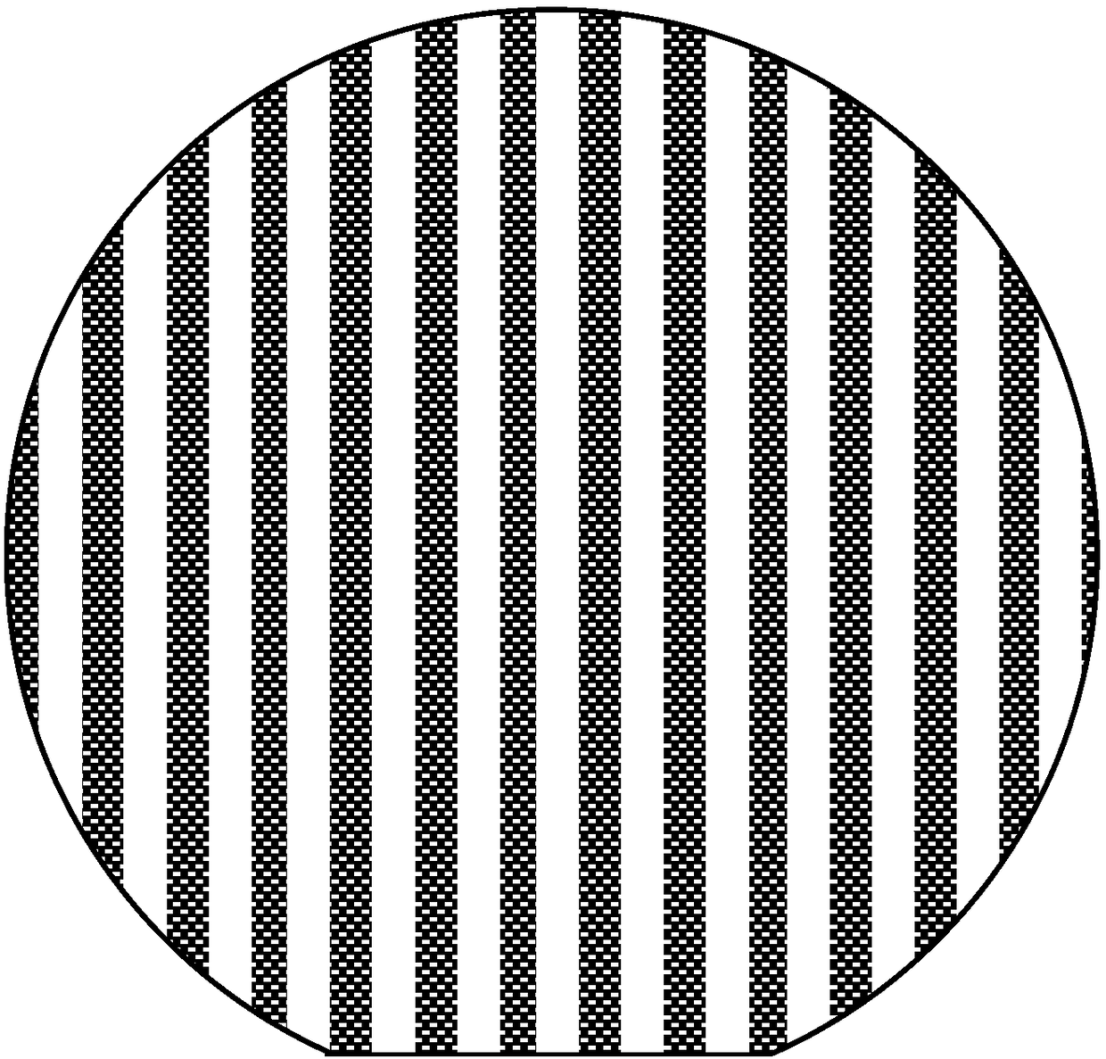
[0074] Step C: Using PECVD plasma enhanced chemical vapor deposition process, the high frequency HF power is 0.43KW, the low frequency LF power is 0.63KW, high-purity SiH 4 The flow rate is 0.23slm, high-purity NH 3 The flow rate is 2.3slm, the flow rate of high-purity nitrogen gas is 2.5slm, the pressure of the reaction chamber is 2.9Torr, and the temperature of the reaction chamber is 400 °C. A compressive stres...


PUM

PropertyMeasurementUnit
thicknessaaaaaaaaaa

Abstract

The invention discloses a manufacturing method for wafer level uniaxial strain GeOI based on a silicon nitride stress membrane and the scale effect. The realization steps are that 1. a germanium-on-insulator GeOI wafer is cleaned, and He ion injection is performed; 2. a pressure stress SiN membrane of more than -1GPa or a tensile stress SiN membrane of more than 1GPa is deposited on the Ge layer of the top layer of the GeOI wafer after ion injection, and the SiN membrane is etched into strip arrays; 3. annealing is performed on the GeOI wafer having the SiN membrane arrays; and 4. the SiN membrane arrays arranged on the surface of the GeOI wafer are removed through corrosion so that the wafer level uniaxial strain GeOI material is obtained. Strain is introduced into the Ge layer of the top layer by utilizing uniaxial tension or uniaxial compressive plastic deformation of an SiO2 buried insulating layer under the effect of the strip SiN membrane arrays. The manufacturing method is compatible with the existing technology, and the required GeOI wafer used for photoelectric integration and system-on-chip can be manufactured.

Description

technical field [0001] The invention belongs to the field of microelectronics technology, and relates to the manufacturing technology of semiconductor substrate materials, specifically a method for manufacturing wafer-level uniaxially strained GeOI materials, which can be used to manufacture GeOI crystals required for optoelectronic integration and system-level chips. round. Background technique [0002] It is well known in the industry that the mobility of electrons and holes of the semiconductor Ge is 2.8 times and 4.2 times that of Si, respectively, and its hole mobility is the highest among all semiconductors. The strained Ge technology that introduces strain technology into Ge-based devices can significantly improve carrier mobility, for example, the hole mobility of strained Ge buried trenches can be increased by 6-8 times. Therefore, Ge and strained Ge will be the best channel materials for Si-based CMOS devices and integrated circuits of 16 nanometers and below. Ge...

Claims


Application Information

Patent Timeline
Patent Type & Authority Patents(China)
IPC IPC(8): H01L21/762
CPCH01L21/7624
Inventor 苗东铭戴显英郝跃祁林林梁彬焦帅
Owner XIDIAN UNIV
Why Eureka
Try Eureka