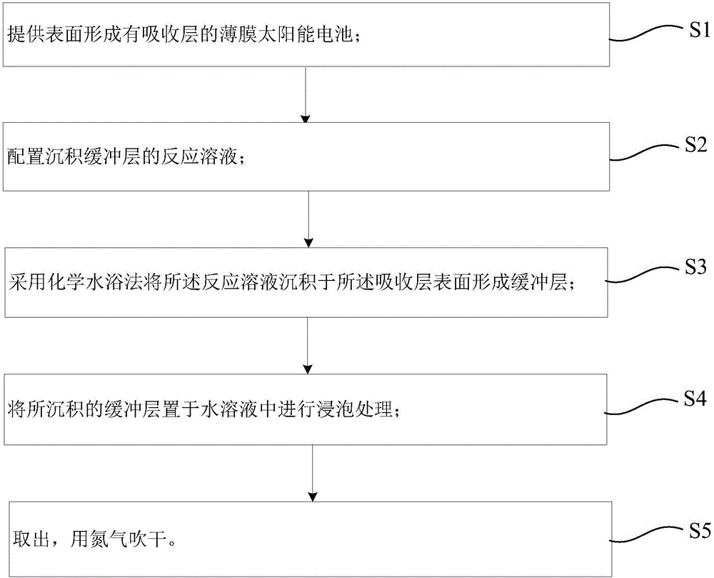
Film solar cell buffer layer postprocessing technology
A technology for solar cells and buffer layers, applied in circuits, photovoltaic power generation, electrical components, etc., can solve the problems of low lattice matching, uneven surface, and many floccules on the surface of the buffer layer, and achieves safe operation and process cost. Low, simple and reliable equipment
- Summary
- Abstract
- Description
- Claims
- Application Information
AI Technical Summary
Problems solved by technology
Method used
Image
Examples
Embodiment 1
[0060] Step 1. Use soda-lime glass as the substrate, perform ultrasonic cleaning, then dry it with pure nitrogen and put it into a magnetron sputtering vacuum chamber, dehydrate and degas, and deposit a double-layer Mo back electrode layer by DC magnetron sputtering, with a thickness of 0.6um;
[0061] Step 2, put the substrate prepared with the Mo back electrode layer into the vacuum chamber, and wait for the vacuum degree to be better than 1×10 -3 After Pa, use CuGa alloy target (Ga content at.25%) and In target to co-sputter to deposit CuInGa (CIG) metal prefabricated layer with a thickness of 0.6um;
[0062] Step 3, put the substrate prepared with the metal prefabricated layer into the selenization furnace, and use H 2 Se was used as a selenium source, selenized at 400°C for 30 minutes, annealed in a nitrogen atmosphere at 580°C for 30 minutes, and then cooled naturally to prepare a CIGS absorbing layer with a thickness of 1.2um;
Embodiment 2
[0069] Step 1. Soda-lime glass is ultrasonically cleaned, then dried with pure nitrogen and placed in a magnetron sputtering vacuum chamber, dehydrated and degassed, and a double-layer Mo back electrode layer is deposited by DC magnetron sputtering, with a thickness of 0.6um;
[0070] Step 2, put the substrate prepared with the Mo back electrode layer into the vacuum chamber, and wait for the vacuum degree to be better than 1×10 -3 After Pa, use CuGa alloy target (Ga content at.25%) and In target to co-sputter to deposit CuInGa (CIG) metal prefabricated layer with a thickness of 0.6um;
[0071] Step 3, put the substrate prepared with the metal prefabricated layer into the selenization furnace, and use H 2 Se was used as a selenium source, selenized at 400°C for 30 minutes, annealed in a nitrogen atmosphere at 580°C for 30 minutes, and then cooled naturally to prepare a CIGS absorbing layer with a thickness of 1.2um;
[0072] Step 4, configure 1.5umol / L zinc sulfate solution, ...
Embodiment 3
[0078] Step 1. Soda-lime glass is ultrasonically cleaned, then dried with pure nitrogen and placed in a magnetron sputtering vacuum chamber, dehydrated and degassed, and a double-layer Mo back electrode layer is deposited by DC magnetron sputtering, with a thickness of 0.6um;
[0079] Step 2, put the substrate prepared with the Mo back electrode layer into the vacuum chamber, and wait for the vacuum degree to be better than 1×10 -3 After Pa, use CuGa alloy target (Ga content at.25%) and In target to co-sputter to deposit CuInGa (CIG) metal prefabricated layer with a thickness of 0.6um;
[0080] Step 3, put the substrate prepared with the metal prefabricated layer into the selenization furnace, and use H 2 Se was used as a selenium source, selenized at 400°C for 30 minutes, annealed in a nitrogen atmosphere at 580°C for 30 minutes, and then cooled naturally to prepare a CIGS absorbing layer with a thickness of 1.2um;
[0081] Step 4, prepare cadmium iodide solution of 1.5umol / ...
PUM
 Abstract
Description
Claims
Application Information
 - R&D
- Intellectual Property
- Life Sciences
- Materials
- Tech Scout
- Unparalleled Data Quality
- Higher Quality Content
- 60% Fewer Hallucinations
Browse by: Latest US Patents, China's latest patents, Technical Efficacy Thesaurus, Application Domain, Technology Topic, Popular Technical Reports.
© 2025 PatSnap. All rights reserved.Legal|Privacy policy|Modern Slavery Act Transparency Statement|Sitemap|About US| Contact US: help@patsnap.com


