Preparation method for field effect transistor

A field-effect transistor and semiconductor technology, applied in the field of electronics, can solve the problems of difficulty in realizing flexibility, large-area devices, unstable electrical performance, and complicated preparation process, and achieves a technology that prevents ultraviolet and electromagnetic radiation, is easy to implement, and has a simple preparation process. Effect

Active Publication Date: 2016-09-07
JIANGSU YOURUN MICROELECTRONICS CO LTD
View PDF3 Cites 8 Cited by
  • Summary
  • Abstract
  • Description
  • Claims
  • Application Information

AI Technical Summary

Problems solved by technology

[0003] However, the existing field effect transistors that can work stably in the atmospheric environment are mostly silicon-based field effect transistors, which will pollute the environment when used in large quantities, the preparation process is complicated, the cost is expensive, and it is not easy to realize flexible and large-area devices; at the same time , the dielectric layer is an important part of the field effect tube.

Method used


Image

  • Preparation method for field effect transistor
  • Preparation method for field effect transistor
  • Preparation method for field effect transistor

Examples


Embodiment 1

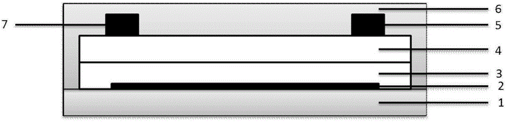
[0047] like figure 1 The bottom gate top contact structure is shown, the material and thickness of each layer are: the substrate is shellac, the gate electrode, source electrode and drain electrode are all silver nanowires, adding 10% shellac and 30% water soluble The adhesive is gelatin, the dielectric layer adopts mica sheet, the thickness is 5nm, the semiconductor layer is zinc oxide, the thickness is 30nm, and the encapsulation layer is shellac. With this structure, a field effect transistor with high lifetime and high stability can be realized.

[0048] The preparation method is as follows:

[0049] ①Clean the mica sheet thoroughly first, then dry it after cleaning;

[0050] ②Preparing the silver nano wire grid electrode 2 on the mica surface by screen printing technology, and curing it;

[0051] ③ Prepare a shellac layer on the grid electrode 2, and rapidly increase the heating temperature of the device to 70°C to 90°C, so that the shellac layer is in a hot-melt state, ...

Embodiment 2

[0058] like figure 1 The bottom gate top contact structure is shown, the material and thickness of each layer are: the substrate is shellac, the gate electrode, source electrode and drain electrode are all aluminum nanowires, and 30% shellac and 30% water soluble The non-toxic adhesive polyvinyl alcohol, the dielectric layer adopts silk fibroin sheet, the thickness is 8nm, the semiconductor layer is graphene oxide, the thickness is 30nm, and the encapsulation layer is shellac. With this structure, a field effect transistor with high lifetime and high stability can be realized.

[0059] Preparation method is like embodiment 1.

Embodiment 3

[0061] like figure 1 Shown is the bottom gate top contact structure, the material and thickness of each layer are: the substrate is shellac, the gate electrode, source electrode and drain electrode are all gold nanowires, adding 30% shellac and 10% water soluble The adhesive is gelatin, the dielectric layer adopts hexagonal boron nitride, the thickness is 10nm, the semiconductor layer is carbon nanotube, the thickness is 50nm, and the encapsulation layer is shellac. With this structure, a field effect transistor with high lifetime and high stability can be realized.

[0062] Preparation method is like embodiment 1.


PUM

PropertyMeasurementUnit
Thicknessaaaaaaaaaa
Thicknessaaaaaaaaaa
Thicknessaaaaaaaaaa

Abstract

The invention discloses a preparation method for a field effect transistor. The field effect transistor comprises a substrate, a gate electrode, a dielectric layer, a semiconductor layer, a source electrode and a drain electrode, and a packaging layer from the bottom up in sequence. Based on the adhesive characteristic of lac, the dielectric material can be physically peeled off so as to form the stable dielectric layer having a thickness equal to that of several molecules, so that a solution method preparation step of the dielectric layer is omitted, the usage of poisonous reagents is effectively eliminated, and the stability is improved; meanwhile, the lac is used as the substrate and the packaging layer; due to the characteristics of high compactness, ultraviolet resistance, radiation resistance and the like of the lac, corrosion to the whole device by water and oxygen can be blocked, and interference on the device by ultraviolet and electromagnetic radiation can be prevented, so that the stability of the overall device is improved and the service life of the overall device is prolonged; the field effect transistor adopts the peelable dielectric layer and the biological material as the substrate and the packaging layer, so that the field effect transistor is easier to prepare and lower in cost; and in addition, the application range of the field effect transistor is expanded, so that the field effect transistor can be applicable to the fields of wearable equipment and bioelectronics, and is suitable for large-scale mass production.

Description

technical field [0001] The invention belongs to the field of electronic technology, in particular to a preparation method of a field effect transistor. Background technique [0002] The performance and production technology of field effect transistors are developing day by day, and the mobility of many new materials exceeds that of amorphous silicon, and they are widely used in electronic paper, sensor identification cards, smart cards and other memory devices. Compared with the traditional silicon-based MOSFET, the device preparation process of the new material field effect transistor replaces the traditional high-temperature vacuum deposition and other methods with simple processes such as low-temperature deposition or solution (black jet printing, spin coating, dripping, etc.) complex process. In addition, the new material itself has the advantages of light weight, low price, flexibility, simple preparation method, various types, and properties that can be adjusted throu...

Claims


Application Information

Patent Timeline
IPC IPC(8): H01L21/336H01L29/78H01L29/423H01L29/49
CPCH01L29/42364H01L29/4966H01L29/66477H01L29/78
Inventor 于军胜庄昕明韩世蛟郑华靖
Owner JIANGSU YOURUN MICROELECTRONICS CO LTD
Why Eureka
Try Eureka