Method for preparing zinc oxide/gallium nitride composite film
A composite film, gallium nitride technology, applied in the field of photocatalysis, can solve the problems of difficult collection and reuse, and achieve the effects of easy reuse, expansion of preparation methods, and obvious visible light response
- Summary
- Abstract
- Description
- Claims
- Application Information
AI Technical Summary
Problems solved by technology
Method used
Image
Examples
Embodiment 1
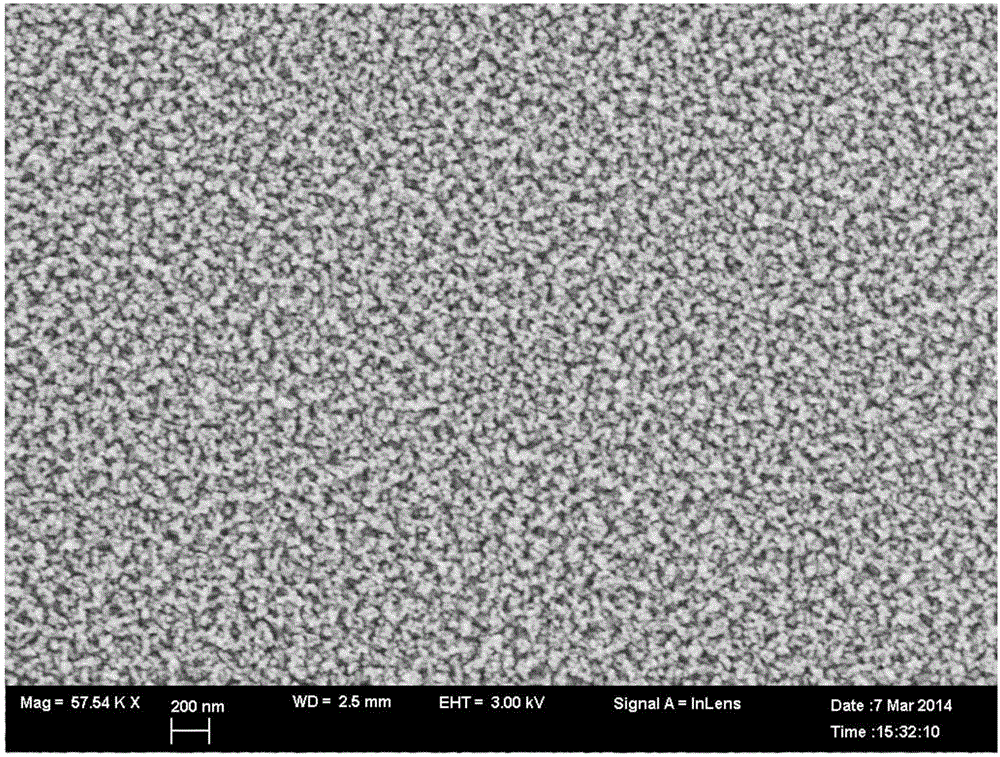
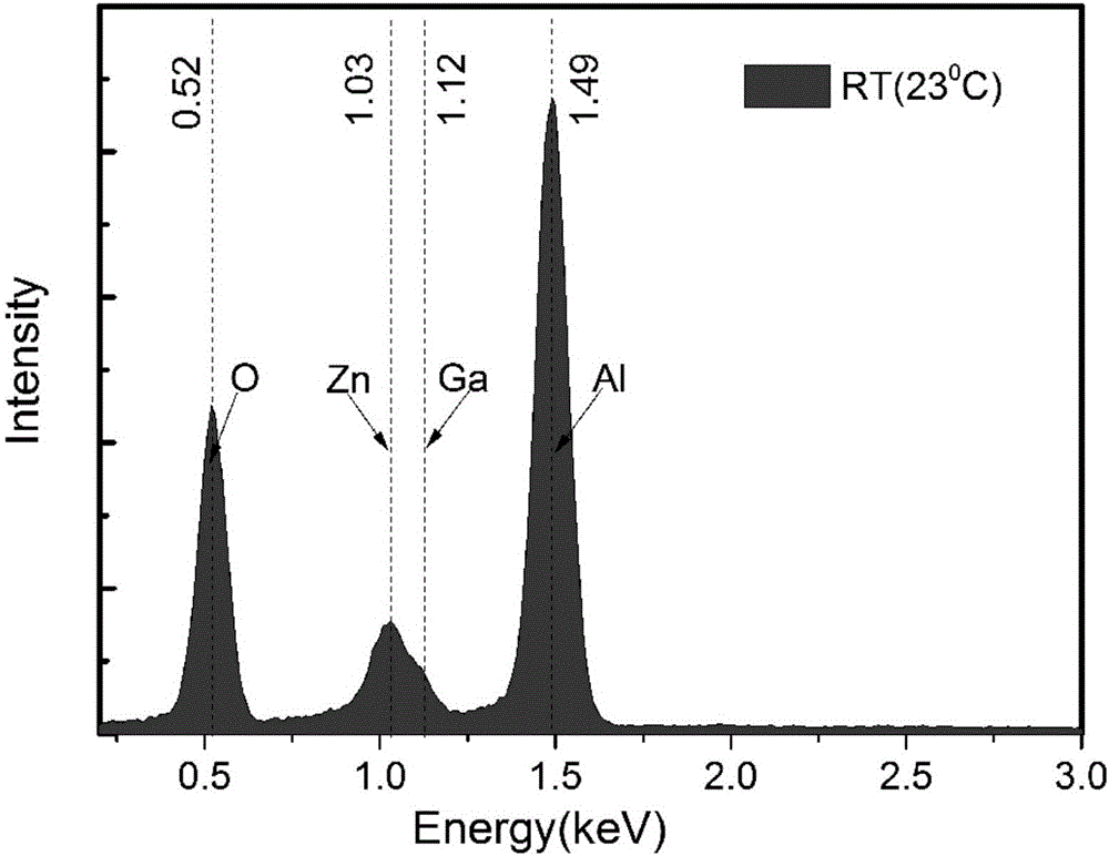
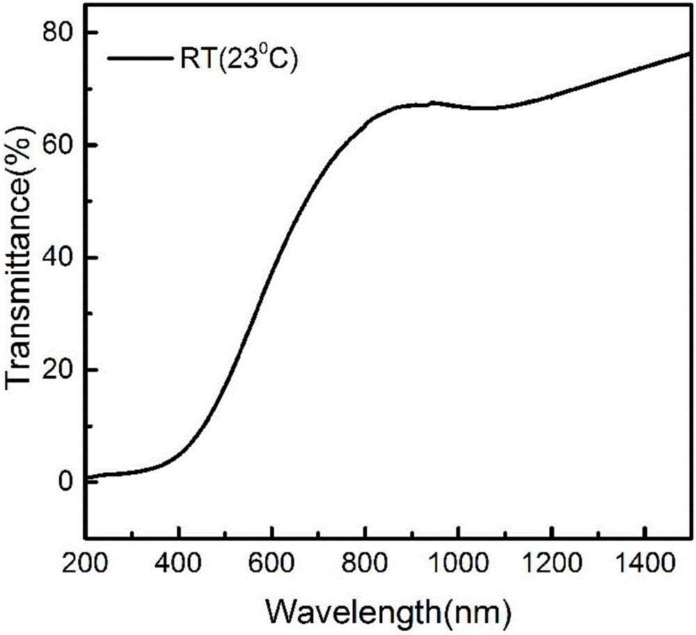
[0024] The sapphire substrate was ultrasonically cleaned in acetone, absolute ethanol and deionized water for 15 minutes, then dried with nitrogen and placed in a vacuum deposition chamber. The experiment adopts the pulse laser deposition method, and the target materials are high-purity zinc oxide and gallium nitride, which are respectively loaded on the target trays at an angle of 30 degrees. The vacuuming of the mechanical pump and the molecular pump makes the vacuum degree of the deposition chamber reach 5×10 -7 Torr. Introduce high-purity nitrogen gas with a gas flow rate of 30 sccm. Let it stand for a period of time so that the vacuum degree in the deposition chamber is stable at 1.2×10 -2 Torr. The deposited substrate temperature was room temperature (23°C). The laser light source is a KrF excimer laser with a laser wavelength of 248nm, a frequency of 3Hz, and a laser energy of 220mJ. The laser is focused on the target through an external focusing lens. The distance...
Embodiment 2
[0029] The substrate deposition temperature in Example 1 was increased from room temperature (23° C.) to 50° C. and kept constant during the deposition. Figure 4 It is the transmission spectrum of the zinc oxide / gallium nitride composite thin film prepared at a substrate temperature of 50°C. It can be seen from the figure that the absorption edge of the transmission has an obvious blue shift compared with that at room temperature, indicating that increasing the deposition temperature The bandgap of the zinc oxide / gallium nitride composite thin film is improved, and its bandgap width is about 1.7eV after analysis.
PUM
| Property | Measurement | Unit |
|---|---|---|
| Band gap width | aaaaa | aaaaa |
| Band gap width | aaaaa | aaaaa |
Abstract
Description
Claims
Application Information


