

Film-substrate micro-through-hole-array biochip and preparation method thereof
A technology of biochip and manufacturing method, which is applied in the field of biological and medical detection, can solve problems such as uneven aperture, single shape, and high price, and achieve the effects of good repeatability, flexible design, and low cost
- Summary
- Abstract
- Description
- Claims
- Application Information
AI Technical Summary
Problems solved by technology
Method used
Image

Examples
Embodiment 1
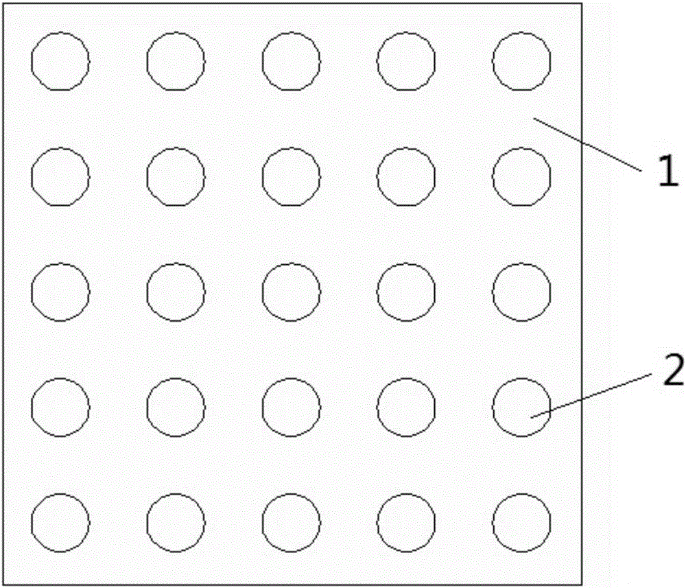
[0025] A kind of PI thin film base microvia array biochip involved in this embodiment is as follows: figure 1 As shown, the structure is as follows:
[0026] The thickness is 10 μm, which is a uniform and transparent PI film 1. The micro-through hole array 2 is distributed on the film 1. The micro-through hole is circular and has a full-through structure. The pore diameter is 8 μm, and the ratio of the pore diameter to the gap between the holes is 1: 1. The micro-via array 2 is arranged in a rectangular distribution. Its scanning electron microscope picture is as Figure 5 shown.
[0027] The flow chart of a method for manufacturing a PI film substrate micro-through-hole array biochip involved in this embodiment is as follows Figure 4 As shown, the steps are as follows:
[0028] (1) In a 500ml beaker, add 239.1g of dimethylacetamide, then add 2.3g of p-phenylenediamine, 24.3g of 4,4'-diaminodiphenyl ether, 21.8g of pyromellitic dianhydride, 12.6 g of pyromellitic dianhyd...
Embodiment 2
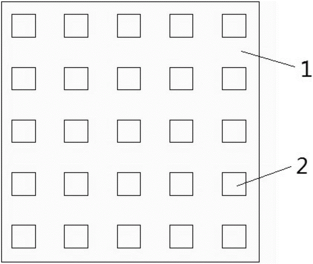
[0033] A kind of PMMA film substrate micro-through-hole array biochip involved in this embodiment is as follows: figure 2 As shown, the structure is as follows:
[0034] It is a uniform and transparent PMMA film 1 with a thickness of 5 μm. Micro-via arrays 2 are distributed on the film 1. The micro-vias are square and have a full-through structure. The diameter of the micro-vias is 4 μm. 1:5, the micro-via array 2 is arranged in a rectangular distribution.
[0035] A flow chart of a method for manufacturing a PMMA film substrate micro-through-hole array biochip involved in this embodiment is as follows Figure 4 As shown, the steps are as follows:
[0036] (1) Take 3g of PMMA particles with an electronic balance, put into a glass bottle filled with 30ml of glacial acetic acid, stir and let stand for 2 hours to obtain a PMMA solution. The PMMA solution was coated on a silicon wafer, the coating speed was 2000 rpm, baked at 150° C. for 20 minutes, thermally cured, and cooled...
Embodiment 3
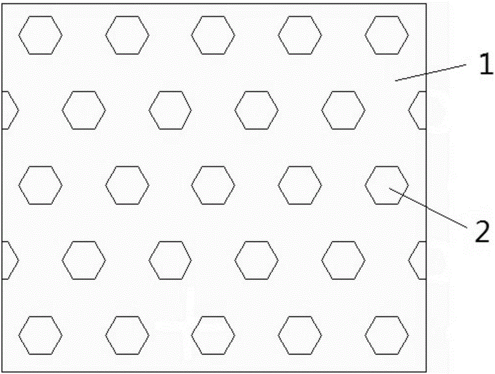
[0041] A kind of PU film substrate micro-through-hole array biochip involved in this embodiment is as follows: image 3 As shown, the structure is as follows:
[0042] It is a uniform and transparent PU film 1 with a thickness of 60 μm. On the film 1 is distributed an array of micro-vias 2 . The micro-vias are regular hexagonal and full-through structures. :10, the micro-via array 2 is arranged in a regular hexagonal distribution.
[0043] The flow chart of a method for manufacturing a PU film substrate micro-through-hole array biochip involved in this embodiment is as follows Figure 4 As shown, the steps are as follows:
[0044] (1) Put 106g of acrylate and 110g of polyethylene glycol into a flask, heat it to 50°C, slowly add 196g of toluene diisocyanate into the flask while stirring, keep it warm for 2 hours, slowly drop to room temperature, add diluent The agent is mixed uniformly to obtain a polyurethane prepolymer. Add the polyurethane prepolymer, acrylate and benzoin ...
PUM
| Property | Measurement | Unit |
|---|---|---|
| Thickness | aaaaa | aaaaa |
| Thickness | aaaaa | aaaaa |
| Thickness | aaaaa | aaaaa |
Abstract
Description
Claims
Application Information