

Efficient copper indium gallium selenide/perovskite series solar cell
A solar cell, copper indium gallium selenide technology, applied in circuits, photovoltaic power generation, electrical components, etc., can solve problems such as the reduction of solar cell efficiency, and achieve the effects of improving energy conversion efficiency, optimizing process parameters, and reducing losses
- Summary
- Abstract
- Description
- Claims
- Application Information
AI Technical Summary
Problems solved by technology
Method used
Image

Examples
Embodiment 1
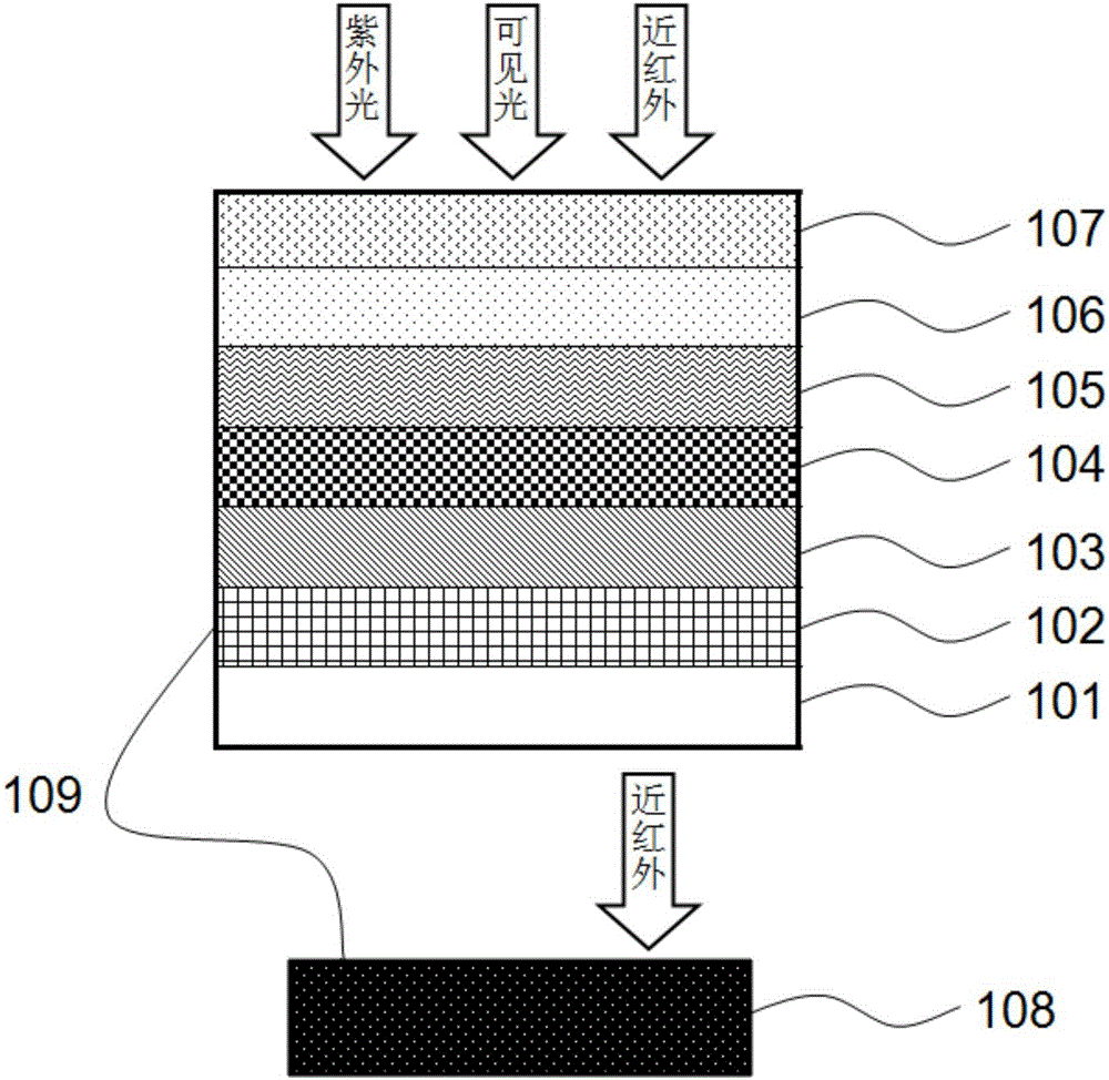
[0036] A high-efficiency copper indium gallium selenide / perovskite tandem solar cell structure such as figure 1 shown. Perovskite solar cells are as follows from bottom to top: transparent substrate 101, first transparent electrode layer 102, hole transport layer 103, perovskite light-absorbing layer 104, electron transport layer 105, second transparent electrode layer 106, Anti-layer 107 . The second transparent electrode layer 106 is sequentially composed of a lower electron extraction layer, an upper electron extraction layer, and a conductive layer from bottom to top. The transparent substrate 101 is quartz glass, the first transparent electrode layer 102 (anode) is ITO, and the thickness is 110nm; the hole transport layer 103 is PEDOT:PSS AI4083, and the thickness is 60nm; the perovskite light-absorbing layer 104 is CH 3 NH 3 PB 3 , with a thickness of 150nm, the electron transport layer 105 is PCBM, with a thickness of 50nm; the lower electron extraction layer is Rho...
Embodiment 2
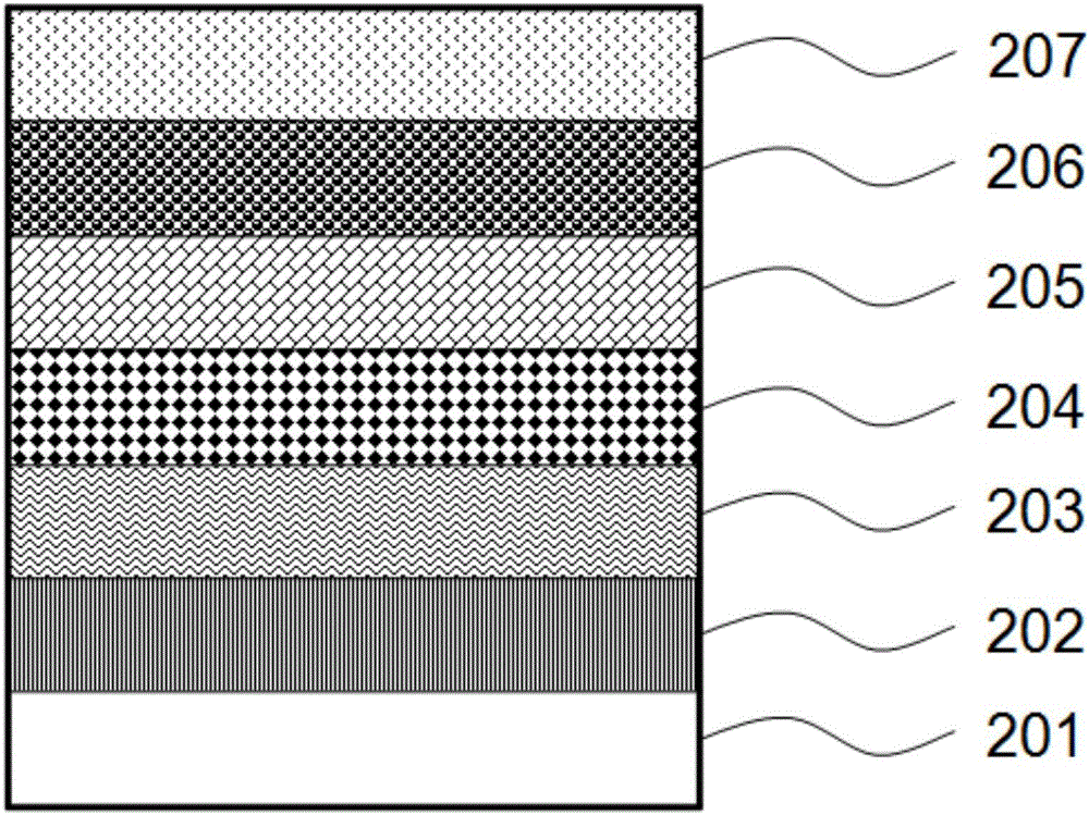
[0044] Perovskite solar cells from bottom to top are: transparent substrate, first transparent electrode layer, hole transport layer, perovskite light absorbing layer, electron transport layer, lower electron extraction layer, upper electron extraction layer, conductive layer, AR layer. The transparent substrate is quartz glass, the first transparent electrode layer (anode) is a three-layer graphene film, each layer thickness is 0.34nm; the hole transport layer is PEDOT:PSS AI4083, the thickness is 60nm; the perovskite light absorption layer is CH 3 NH 3 PB 3-X Cl X , the thickness is 160nm; the electron transport layer is PCBM, the thickness is 50nm; the lower electron extraction layer is Rhodamine101, the thickness is 0.5nm; the upper electron extraction layer is LiF, the thickness is 0.5nm; the conductive layer is ultra-thin Ag, the thickness is 8nm; The anti-reflection layer is MoO X , with a thickness of 2 nm.
[0045] Copper indium gallium selenide solar cells from ...
Embodiment 3
[0051] Perovskite solar cells from bottom to top are: transparent substrate, first transparent electrode layer, electron transport layer, perovskite light-absorbing layer, hole transport layer, second transparent electrode layer, and antireflection layer. The transparent substrate is quartz glass, the first transparent electrode layer (cathode) is FTO with a thickness of 100nm; the electron transport layer is ZnO nano film with a thickness of 40nm; the perovskite light-absorbing layer is CH 3 NH 3 PB 3 , the thickness is 160nm; the hole transport layer is PTAA, the film thickness is 50nm; the second transparent electrode layer (anode) is ultra-thin Ag, the thickness is 12nm; the anti-reflection layer is MoO X , with a thickness of 2 nm.
[0052] Copper indium gallium selenide solar cells from bottom to top are: with SiO 2 layer glass substrate; the anode is Mo, the thickness is 800nm; the copper indium gallium selenide absorbing layer, the thickness is 2um; the buffer layer...
PUM
 Abstract
Description
Claims
Application Information