led epitaxial growth method

A technology of epitaxial growth and growth temperature, applied in semiconductor devices, electrical components, circuits, etc., can solve problems such as low activation rate of dopants, lattice mismatch, and poor crystal quality of materials

Active Publication Date: 2018-10-02
XIANGNENG HUALEI OPTOELECTRONICS
View PDF4 Cites 0 Cited by
  • Summary
  • Abstract
  • Description
  • Claims
  • Application Information

AI Technical Summary

Problems solved by technology

[0003] In the InGaN / GaN-based light-emitting diode (LED) material structure, the p-AlGaN layer is usually located between the quantum well and the p-type GaN. Under injection conditions, electrons overflow quantum wells and cause problems such as a decrease in luminous efficiency
In general, there are many difficulties in the growth of p-AlGaN layer, such as poor material crystal quality, lattice mismatch and low dopant activation rate, etc., and the doping efficiency of p-AlGaN layer is low, and hole injection is insufficient

Method used


Image

  • led epitaxial growth method
  • led epitaxial growth method
  • led epitaxial growth method

Examples


Embodiment 1

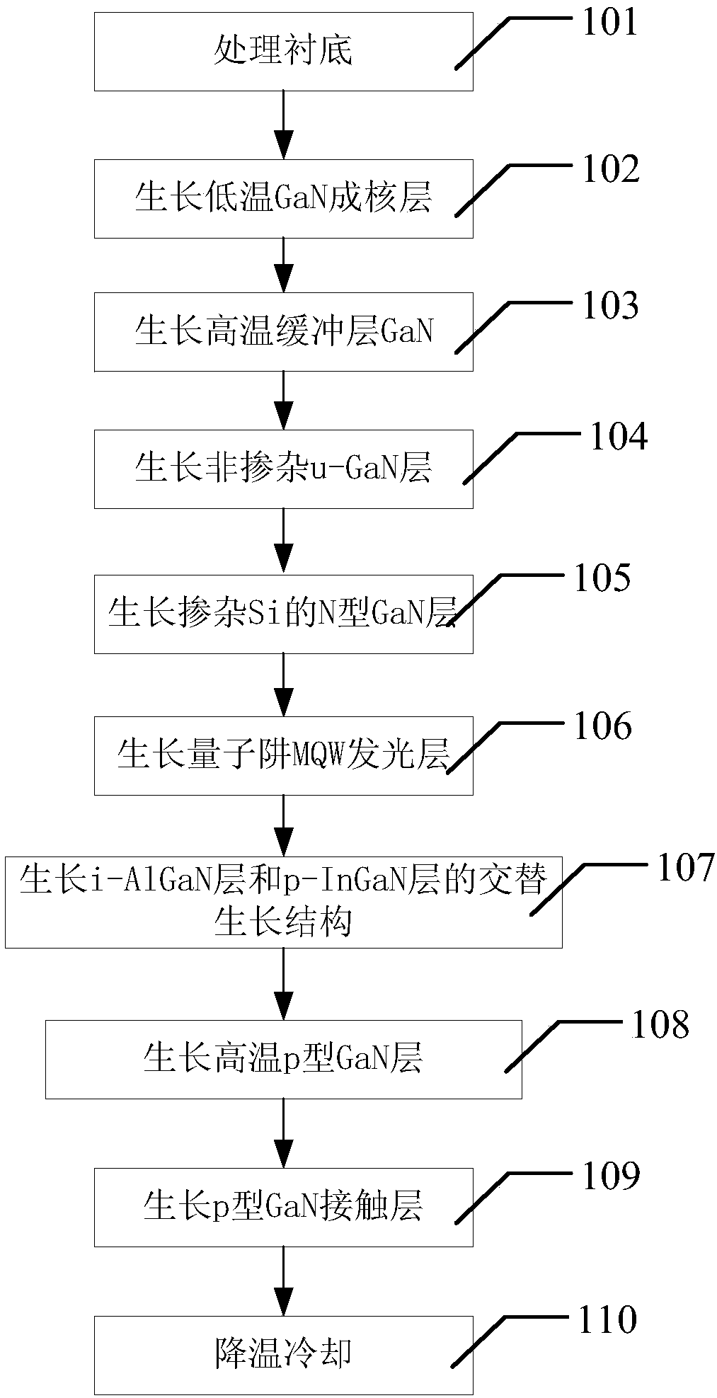
[0051] The invention uses VEECO MOCVD to grow high-brightness GaN-based LED epitaxial wafers. Using high-purity H 2 or high purity N 2 (purity 99.999%) mixed gas as carrier gas, high-purity NH 3 (purity 99.999%) as N source, metal-organic source trimethylgallium (TMGa) as gallium source, trimethylindium (TMIn) as indium source, and N-type dopant as silane (SiH 4 ), trimethylaluminum (TMAl) as the aluminum source, and the P-type dopant as magnesium dicene (CP 2 Mg), the substrate is (001) sapphire, and the reaction pressure is between 100Torr and 1000Torr. The specific growth method is as follows:

[0052] A kind of LED epitaxial growth method, see figure 1 , including: processing the substrate, growing a low-temperature GaN nucleation layer, growing a high-temperature buffer layer GaN, growing an undoped u-GaN layer, growing a Si-doped n-GaN layer, growing a light-emitting layer, and growing a high-temperature p-type GaN layer , growing a p-type GaN contact layer, coolin...

Embodiment 2

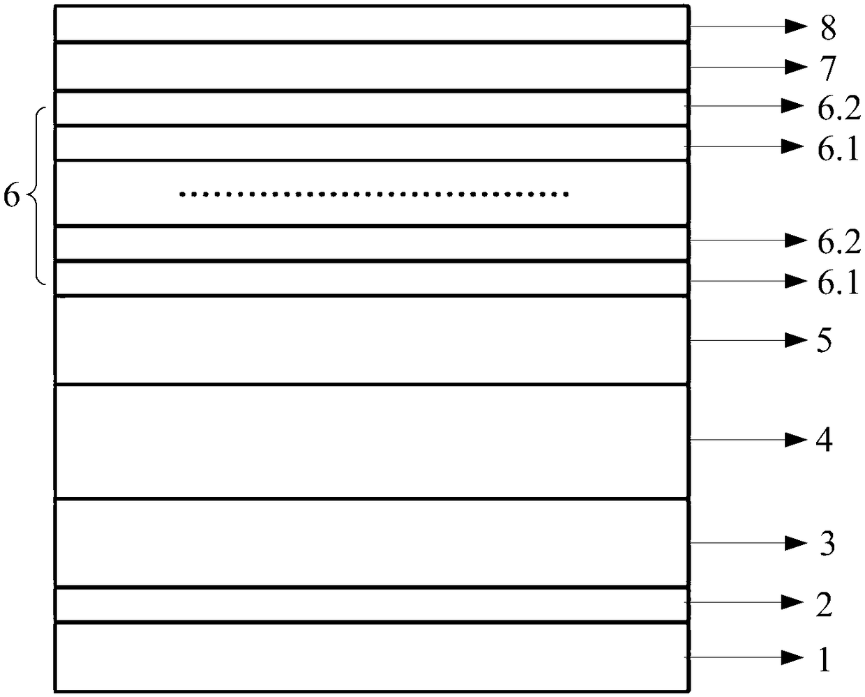
[0062] The application examples of the LED epitaxial growth method of the present invention are provided below, and its epitaxial structure can be found in figure 2 , growth method see figure 1 . Using VEECO MOCVD to grow high-brightness GaN-based LED epitaxial wafers. Using high-purity H 2 or high purity N 2 or high purity H 2 and high purity N 2 The mixed gas as the carrier gas, high-purity NH 3 As the N source, the metal-organic source trimethylgallium (TMGa) is used as the gallium source, trimethylindium (TMIn) is used as the indium source, and the N-type dopant is silane (SiH 4 ), trimethylaluminum (TMAl) as the aluminum source, and the P-type dopant as magnesium dicene (CP 2 Mg), the substrate is (0001) sapphire, and the reaction pressure is between 100torr and 1000torr. The specific growth method is as follows:

[0063] Step 101, processing the substrate:

[0064] The sapphire substrate is annealed in a hydrogen atmosphere to clean the surface of the substrat...

Embodiment 3

[0092] A conventional LED epitaxial growth method is provided below as a comparative example of the present invention.

[0093] The growth method of conventional LED epitaxy is (see the epitaxial layer structure image 3 ):

[0094] 1. Anneal the sapphire substrate in a hydrogen atmosphere to clean the surface of the substrate at a temperature of 1050-1150°C.

[0095] 2. Lower the temperature to 500-620°C and feed NH 3 and TMGa, grow a 20-40nm thick low-temperature GaN nucleation layer at a growth pressure of 400-650Torr.

[0096] 3. After the growth of the low-temperature GaN nucleation layer is completed, stop feeding TMGa and perform in-situ annealing treatment. The annealing temperature is increased to 1000-1100°C, and the annealing time is 5-10min; after annealing, adjust the temperature to 900-1050°C , continue to pass through TMGa, and epitaxially grow a high-temperature GaN buffer layer with a thickness of 0.2-1um, and a growth pressure of 400-650Torr.

[0097] 4. ...


PUM


Abstract

The invention discloses an LED epitaxial growth method. The LED epitaxial growth method comprises the following steps in sequence: processing a substrate, growing a low-temperature GaN nucleating layer, growing a high-temperature GaN buffer layer, growing a non-doped u-GaN layer, growing an Si-doped n-GaN layer, growing a luminous layer, growing an i-AlGaN layer and p-InGaN layer alternated growth structure, growing a high-temperature p-type GaN layer, growing a p-type GaN contact layer and cooling. Through the scheme, a traditional LED epitaxial electron blocking layer is designed into a low-voltage high-temperature i-AlGaN layer and high-voltage low-temperature p-InGaN layer alternated layer growth structure, an electron blocking effect is reached, and the increase of hole injection level is also facilitated, so that the luminous efficiency of an LED is improved.

Description

technical field [0001] The present application relates to the technical field of LED epitaxial design application, and in particular, relates to an LED epitaxial growth method. Background technique [0002] At present, LED (Light Emitting Diode, light-emitting diode) is a kind of solid-state lighting. Its advantages such as small size, low power consumption, long service life, high brightness, environmental protection, and durability are recognized by consumers, and the scale of domestic production of LEDs is gradually expanding. ;The demand for LED brightness and luminous efficiency is increasing day by day in the market. What customers are concerned about is that LEDs are more power-saving, have higher brightness and better luminous efficiency, which puts forward higher requirements for LED epitaxial growth; how to grow better epitaxial wafers It has been paid more and more attention because the performance of LED devices can be improved due to the improvement of the cryst...

Claims


Application Information

Patent Timeline
Patent Type & Authority Patents(China)
IPC IPC(8): H01L33/00H01L33/14H01L33/32
CPCH01L33/0075H01L33/145H01L33/32
Inventor 徐平林传强
Owner XIANGNENG HUALEI OPTOELECTRONICS
Why Eureka
Try Eureka