Silicon-doped gallium nitride nanoribbon ultraviolet detector and preparation method thereof

A gallium nitride nanometer and silicon-doped technology, which is applied in semiconductor devices, final product manufacturing, sustainable manufacturing/processing, etc., can solve the problems of long transmission distance of photogenerated carriers, low optical gain, and low optical switching ratio

Active Publication Date: 2016-12-14
SOUTH CHINA NORMAL UNIVERSITY
View PDF3 Cites 11 Cited by
  • Summary
  • Abstract
  • Description
  • Claims
  • Application Information

AI Technical Summary

Problems solved by technology

[0004] The traditional layered gallium nitride ultraviolet photodetector acceptor material has many dislocations, the crystal quality is poor, and the photogenerated carrier has a long transmission distance in the bulk material. Low gain and poor switching characteristics limit the applica

Method used


Image

  • Silicon-doped gallium nitride nanoribbon ultraviolet detector and preparation method thereof
  • Silicon-doped gallium nitride nanoribbon ultraviolet detector and preparation method thereof
  • Silicon-doped gallium nitride nanoribbon ultraviolet detector and preparation method thereof

Examples


preparation example Construction

[0035] The invention provides a method for preparing a silicon-doped gallium nitride nanobelt ultraviolet light detector, comprising the following steps:

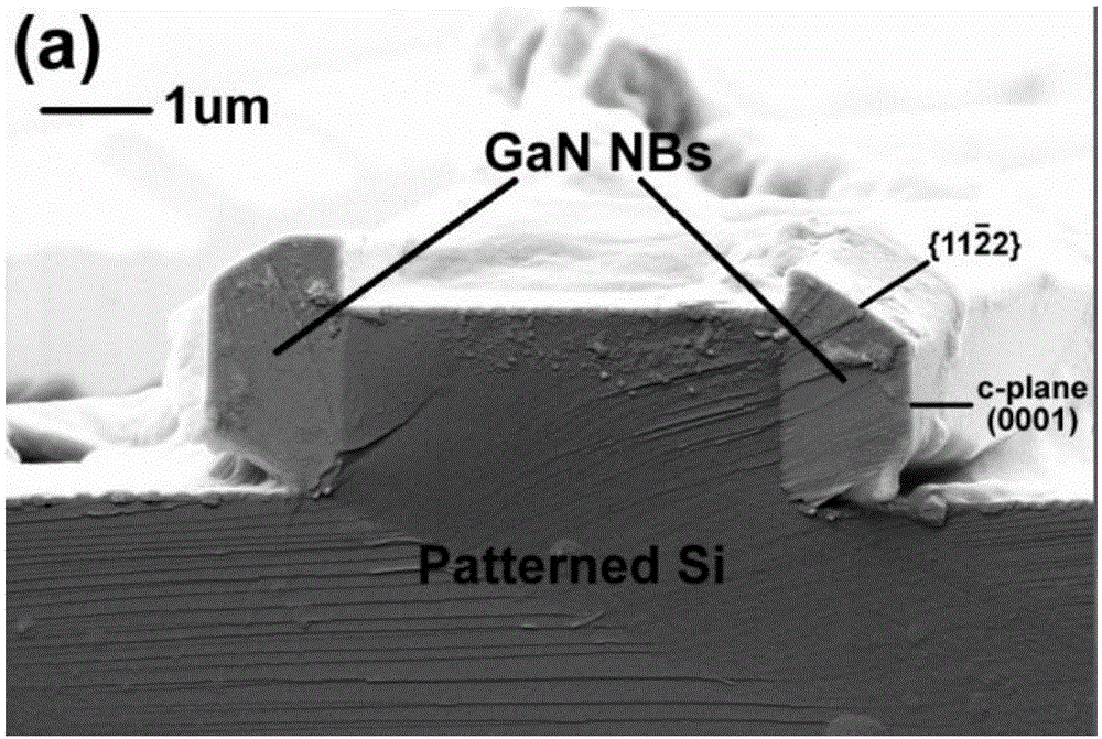
[0036] (1) Photoetching and potassium hydroxide wet etching patterns on a silicon substrate coated with silicon dioxide as a mask;

[0037] (2) growing silicon-doped gallium nitride nanobelts on the groove sidewalls of the pattern;

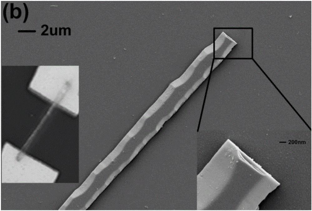
[0038] (3) peeling off the nanobelt, and transferring the peeled nanobelt to a silicon wafer substrate coated with silicon dioxide;

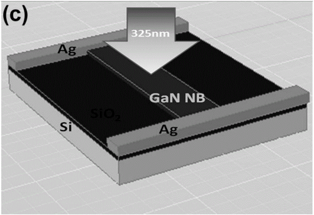
[0039] (4) silver-plated electrodes are plated on the nanobelts of the substrate obtained in the step (3) to obtain a silicon-doped gallium nitride nanobelt ultraviolet light detector.

[0040] In the invention, patterns are photoetched on a silicon substrate plated with silicon dioxide as a mask. In the present invention, the resistivity of the silicon substrate coated with silicon dioxide as a mask is preferably greater than 1000Ω·cm, more preferably greater ...

Embodiment 1

[0056] 1) Photolithography and potassium hydroxide wet etching patterns on a silicon substrate plated with 150nm silicon dioxide as a mask, with a crystal orientation of , a resistivity of 1000Ω·cm, and a thickness of 420μm, to obtain a pattern It is an array of striped grooves with a width of 5.5 μm and a depth of 2 μm, with side walls vertical and parallel to each other. The array of stripe grooves is parallel to the silicon substrate. The crystal orientation, the groove pitch is 4.5μm.

[0057] 2) Using a metal organic compound vapor deposition system to grow silicon-doped gallium nitride nanobelts on the groove sidewall of the patterned silicon substrate obtained in step 1); the silicon doping concentration is 1×10 18 cm- 3 , the nanobelts were grown with a thickness of 0.8 μm.

[0058] 3) Stripping the nanoribbons grown on the silicon substrate in step 2) with a solution having a volume ratio of nitric acid:hydrofluoric acid:water=5:2:1.

[0059] 4) Dissolve the nanob...

Embodiment 2

[0066] 1) On a silicon substrate plated with 100nm silicon dioxide as a mask, the crystal orientation is , the resistivity is 1100Ω·cm, and the thickness is 440μm, the pattern is obtained by photolithography and potassium hydroxide wet etching It is an array of striped grooves with a width of 5.5 μm and a depth of 2 μm, with side walls vertical and parallel to each other. The array of stripe grooves is parallel to the silicon substrate. The crystal orientation, the groove pitch is 4.5μm.

[0067] 2) Using a metal organic compound vapor deposition system to grow silicon-doped gallium nitride nanobelts on the groove sidewall of the patterned silicon substrate obtained in step 1); the silicon doping concentration is 2×10 18 cm- 3 , the nanoribbons were grown with a thickness of 1.2 μm.

[0068] 3) Stripping the nanoribbons grown on the silicon substrate in step 2) with a solution having a volume ratio of nitric acid:hydrofluoric acid:water=5:2:1.

[0069] 4) Dissolve the nano...


PUM

PropertyMeasurementUnit
Resistivityaaaaaaaaaa
Thicknessaaaaaaaaaa
Widthaaaaaaaaaa

Abstract

The invention provides a silicon-doped gallium nitride nanoribbon ultraviolet detector and a preparation method thereof. The method comprises the following steps: (1) performing pattern photoetching and potassium hydroxide wet etching on a silicon substrate which is plated with silicon dioxide serving as a mask; (2) growing a silicon-doped gallium nitride nanoribbon on the groove side wall of the pattern; (3) peeling the nanoribbon, and transferring the peeled nanoribbon to the silicon dioxide plated silicon wafer substrate; and (4) plating a silver electrode on the nanoribbon of the substrate obtained in the step (3) so as to obtain the silicon-doped gallium nitride nanoribbon ultraviolet detector. According to the technical scheme, the photoswitch ratio and optical gain of a micro/nano measurement gallium nitride ultraviolet detector can be improved. Experimental results indicate that the silicon-doped gallium nitride nanoribbon ultraviolet detector has a photoswitch ratio of 5.4*10<4>, optical gain and optical sensitivity of 8.8*10<5> and 2.3*10<-5>A/W respectively.

Description

technical field [0001] The invention relates to the technical field of nano-gallium nitride material ultraviolet detectors, in particular to a silicon-doped gallium nitride nanobelt ultraviolet detector and a preparation method thereof. Background technique [0002] In recent years, with the extension of material science research from high-dimensional to low-dimensional, one-dimensional nanomaterials such as nanowires and nanoribbons exhibit large surface-to-volume ratios, high crystal quality, and many optical properties different from bulk materials. And electrical properties, which has aroused people's strong research interest. [0003] Gallium nitride (GaN) material is an ideal short-wavelength light-emitting device material. The band gap of GaN and its alloys covers the spectral range from infrared to ultraviolet. Gallium nitride is an ideal material for making ultraviolet light detectors because of its suitable band gap (3.4eV) and stable chemical properties. [0004...

Claims


Application Information

Patent Timeline
IPC IPC(8): H01L31/18
CPCH01L31/1804Y02P70/50
Inventor 李述体赵亮亮王幸福
Owner SOUTH CHINA NORMAL UNIVERSITY
Why Eureka
Try Eureka