Method for preparing p-type AlGaN/AlInGaN electron blocking layer near ultraviolet LED with doping density and Al component in stepwise change

A technology of electron blocking layer and doping concentration, which is applied in the direction of circuits, electrical components, semiconductor devices, etc., and can solve the problem that the output power is only the input power, etc.

Active Publication Date: 2017-01-04
东莞市中晶半导体科技有限公司
View PDF8 Cites 20 Cited by
  • Summary
  • Abstract
  • Description
  • Claims
  • Application Information

AI Technical Summary

Problems solved by technology

The photoelectric conversion efficiency of ultraviolet LEDs with a wavelength above 385nm is significantly improved compared to short wavelengths, but the output power is only 15% of the input power

Method used


Image

  • Method for preparing p-type AlGaN/AlInGaN electron blocking layer near ultraviolet LED with doping density and Al component in stepwise change

Examples


Embodiment 1

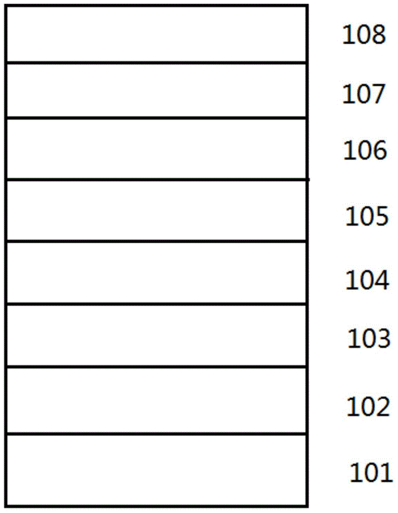
[0019] Using Aixtron’s close-coupled vertical reaction chamber MOCVD growth system, trimethylgallium (TMGa), triethylgallium, trimethylaluminum, trimethylindium and ammonia were used as Ga, Al, In and N source, silane (SiH 4 ) as an n-type dopant source, dimagnesocene (Cp 2 Mg) as a p-type dopant source, the patterned Al 2 o 3 The substrate 101 is heated to 1080-1100 degrees centigrade, and the pressure in the reaction chamber is 100 torr. 2 Under treatment for 5 minutes, then cool down to 530-550 degrees Celsius in the patterned Al 2 o 3 On the substrate 101, the pressure of the reaction chamber is 500 torr, the hydrogen (H2) atmosphere, the V / III molar ratio is 500-1300, and the low-temperature GaN nucleation layer 102 after three-dimensional growth of 20-30 nm is reacted at 1000-1500 ° C The chamber pressure is 200-300torr, in hydrogen (H 2 ) atmosphere, the V / III molar ratio is 1000-1300; grow a high-temperature non-doped GaN buffer layer 103 with a thickness of 2-4 ...


PUM


Abstract

The invention provides a method for preparing a p-type AlGaN/AlInGaN electron blocking layer near ultraviolet LED with doping density and Al component in stepwise change. In an LED epitaxial structure, an electron blocking layer adopts a p-type Aly1Ga1-y1N/AlyInx1Ga1-x1N superlattice structure, and the Al component is reduced from 0.2 to 0.05 stepwisely with the increase of superlattice cycle number; Mg doping density increases stepwisely with the increase of superlattice cycle number, and corresponding hole concentration increases from 0.5*10<17> cm<3> to 2* 10<17> cm<3>; the thickness range of the AlGaN barrier layer is 2-5 nm; and the thickness of the GaN well layer is 2 nm-5 nm. Through the design of the novel ultraviolet LED electronic blocking layer structure, hole injection efficiency can be improved effectively, and electron-hole recombination luminescence efficiency is improved, and thus near ultraviolet LED luminescence efficiency is improved.

Description

technical field [0001] The present invention relates to the technical field of semiconductor optoelectronics, a method for manufacturing a near-ultraviolet light-emitting diode, in particular to a p-type AlGaN / AlInGaN whose doping concentration and Al composition are changed stepwise by using MOCVD (metal organic compound vapor phase epitaxy) technology Electron blocking layer approach for near-ultraviolet LEDs. Background technique [0002] Ultraviolet semiconductor light sources are mainly used in biomedicine, anti-counterfeiting identification, purification (water, air, etc.), computer data storage, and military affairs. With the advancement of ultraviolet light technology, new applications will continue to appear to replace the original technology and products, and ultraviolet light LEDs have broad market application prospects. The ultraviolet light source will be developed for general lighting, optical tweezers, plant growth, oil pipeline leak detection, archaeological...

Claims


Application Information

Patent Timeline
Patent Type & Authority Applications(China)
IPC IPC(8): H01L33/00H01L33/14
CPCH01L33/007H01L33/145
Inventor 贾传宇殷淑仪张国义
Owner 东莞市中晶半导体科技有限公司
Why Eureka
Try Eureka