N-type crystalline silicon double-sided solar cell structure and preparation method thereof

A technology for solar cells and crystalline silicon, applied in the field of solar cells, can solve the problems of no application, increased process complexity, unsuitable for industrialized production of N-type crystalline silicon cells, etc. small effect

Active Publication Date: 2017-02-15
LONGI SOLAR TECH (TAIZHOU) CO LTD
View PDF6 Cites 16 Cited by
  • Summary
  • Abstract
  • Description
  • Claims
  • Application Information

AI Technical Summary

Problems solved by technology

There are also electrode production methods such as photolithography, electroplating, LIP, and inkjet. Although relatively thin fine grid lines can be produced, it also greatly increases the complexity of the process, so it is not suitable for the industrialization of N-type crystalline silicon cells. Production
There are also people who combine metal filaments with silicon substrates or local metal electrodes through conductive adhesives to replace traditional thin grid lines, but these electrode manufacturing methods are not used in the electrodes of N-type crystalline silicon double-sided solar cells. get applied

Method used


Image

  • N-type crystalline silicon double-sided solar cell structure and preparation method thereof
  • N-type crystalline silicon double-sided solar cell structure and preparation method thereof
  • N-type crystalline silicon double-sided solar cell structure and preparation method thereof

Examples


Embodiment 1

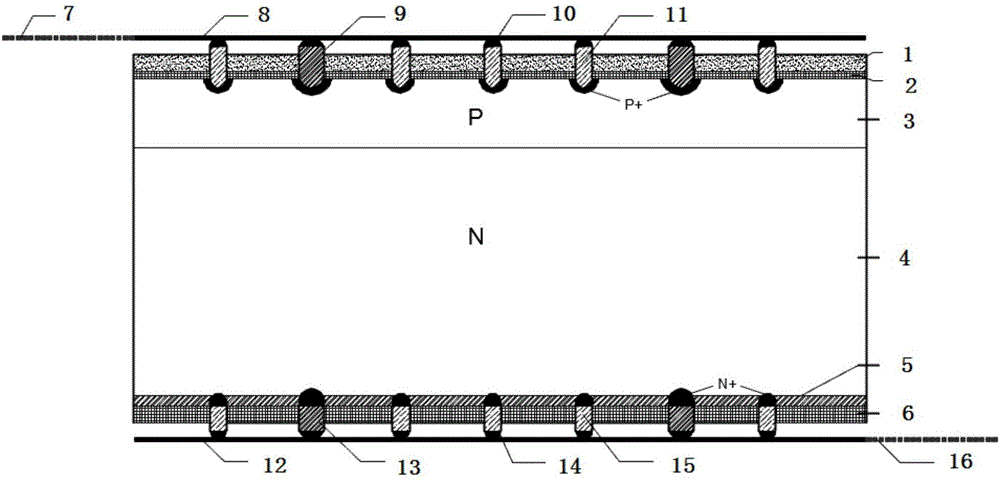
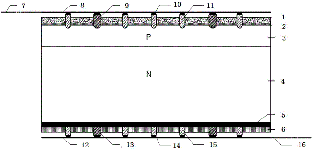
[0067] (1) The N-type monocrystalline silicon wafer is anisotropically etched in a KOH solution at about 80°C to obtain a pyramid structure on the surface.

[0068] (2) On the front side of the silicon wafer, with BBr 3 As an impurity, it is diffused at a low pressure at about 950°C to form a uniform diffusion layer of 40Ω / □.

[0069] (3) On the back of the silicon wafer, POCl 3 As an impurity, it is diffused under low pressure at about 800°C to form a uniform diffusion layer of 40Ω / □.

[0070] (4) Spray a mask on the front and back of the silicon wafer according to a specific pattern. The pattern of the front and back masks is a combination of four equidistant main grids and arrayed line segments, where the width of a single line segment is 40um, the length is 0.5mm, and the distance between two adjacent line segments in the same row is 0.5mm. The distance between two adjacent line segments in the same column is 1.5mm. The busbar has a width of 1.2mm and a length of 156mm...

Embodiment 2

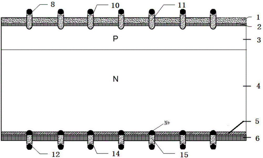
[0082] (1) N-type monocrystalline silicon wafers are anisotropically etched in a KOH solution at about 80°C to obtain a pyramid structure on the surface.

[0083] (2) Coating boron paste on the front side of the silicon wafer.

[0084] (3) Dry the boron paste on the front side of the silicon wafer.

[0085] (4) Print phosphor paste on the back of the silicon wafer according to a specific pattern. The printed pattern is a line segment distributed in an array. The width of a single line segment is 50um and the length is 3mm. The distance between two adjacent line segments in the same row is 2mm. The distance between two adjacent line segments is 3mm.

[0086] (5) Dry the phosphorous slurry in the local area on the back of the silicon wafer.

[0087] (6) Heat treatment at about 950°C to diffuse boron atoms on the front of the silicon wafer and phosphorus atoms on the back to the silicon substrate, thereby forming a uniform P-type diffusion layer of 100Ω / □ on the front of the si...

Embodiment 3

[0099] (1) N-type monocrystalline silicon wafers are anisotropically etched in NaOH solution at about 80°C to obtain a surface pyramid structure.

[0100] (2) Boron atoms are doped on the front side of the N-type silicon wafer by ion implantation, and the boron source is BF 3 , forming a uniform diffusion layer of 80Ω / □.

[0101] (3) Phosphorus atoms are doped on the back of the N-type silicon wafer by ion implantation, and the boron source is PH 3 , forming a uniform diffusion layer of 70Ω / □.

[0102] (4) Chemically cleaning the silicon wafer after ion implantation.

[0103] (5) Aluminum oxide of about 3nm is deposited on the front, and then silicon nitride of about 80nm is deposited; silicon nitride of about 80nm is deposited on the back.

[0104] (6) On the front side of the silicon wafer, use screen printing method to prepare partial contact metal electrodes on the front side according to the array distribution pattern. The printed pattern is a dot array, the diameter o...


PUM

PropertyMeasurementUnit
lengthaaaaaaaaaa

Abstract

The invention discloses an N-type crystalline silicon double-sided solar cell structure and a preparation method thereof. The N-type crystalline silicon double-sided solar cell structure sequentially comprises a front metal wire, a front local contact metal electrode, a front antireflection film, a front passivation film, a P-type doped layer, an N-type crystalline silicon substrate, an N+ region, a back passivation film, a back local contact metal electrode and a back metal wire from top to bottom, wherein fine metal wires are combined with the local contact metal electrodes through a conductive bonded material to form a conductive assembly capable of replacing a fine grid line of a battery. A main grid line or an electrode lead exports current collected on the front surface and the back surface of the battery. Due to the structure of the battery, the contact area of metal and the silicon substrate is reduced, the composite loss is reduced, the light shading area of the grid lines is significantly reduced, so that the conversion efficiency of the battery is improved, and meanwhile, the production cost is reduced by reducing the dosage of silver paste.

Description

technical field [0001] The invention belongs to the technical field of solar cells, in particular to an N-type crystalline silicon double-sided solar cell structure and a preparation method thereof. Background technique [0002] Since the first solar cell was born in Bell Laboratories in 1954, crystalline silicon solar cells have been widely used, the conversion efficiency has been continuously improved, and the production cost has continued to decline. At present, crystalline silicon solar cells account for more than 80% of the total global solar cell market, and the conversion efficiency of crystalline silicon cell production lines has exceeded 20%. The cost of electricity continues to shrink and is expected to be flat in the next few years. As a clean energy source, crystalline silicon solar cells play an increasingly important role in changing the energy structure and alleviating environmental pressure. [0003] According to the doping type of the substrate, crystallin...

Claims


Application Information

Patent Timeline
Patent Type & Authority Applications(China)
IPC IPC(8): H01L31/068H01L31/0224H01L31/18
CPCH01L31/022433H01L31/0684H01L31/1804Y02E10/547Y02P70/50
Inventor 李华钟宝申赵科雄
Owner LONGI SOLAR TECH (TAIZHOU) CO LTD
Why Eureka
Try Eureka