Zn: Ga2O3 film-based MSM structure solar-blind ultraviolet photoelectric detector and preparation method thereof
An electrical detector and ultraviolet light technology, applied in the field of photodetectors, can solve the problem of reducing the response time of photodetectors, and achieve the effects of easy operation, stable and uniform thickness, and strong process controllability
- Summary
- Abstract
- Description
- Claims
- Application Information
AI Technical Summary
Problems solved by technology
Method used
Image
Examples
example 1
[0023] Example 1: Pure Ga 2 o 3 Fabrication of thin-film solar-blind photodetectors
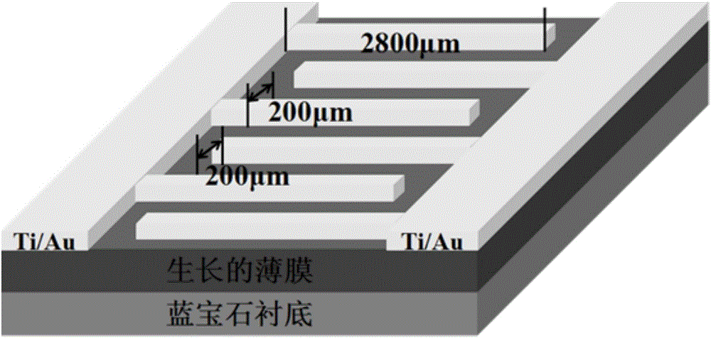
[0024] First take a c-plane sapphire substrate with a size of 10mm×10mm×0.5mm, soak the substrate in acetone, ethanol, and deionized water for 10 minutes, then rinse it with deionized water after taking it out, and finally wash it with dry N 2Blow dry and set aside. Put the above-mentioned cleaned sapphire substrate into the deposition chamber, and grow a layer of 200nm β-Ga on it by magnetron sputtering 2 o 3 thin film, with 99.99% pure Ga 2 o 3 The ceramic is used as the target material, and the specific growth parameters of the film are as follows: the background vacuum is 1×10 - 4 Pa, the working atmosphere is Ar gas, the working pressure is 0.8Pa, the substrate temperature is 650°C, the sputtering power is 80W, and the sputtering time is 2h. The β-Ga prepared above 2 o 3 The thin film is covered with a hollow interdigitated electrode mask, and the metal Ti layer (30nm) and Au l...
example 2
[0025] Example 2: Zn:Ga doped with different concentrations of Zn 2 o 3 Fabrication of thin-film solar-blind photodetectors
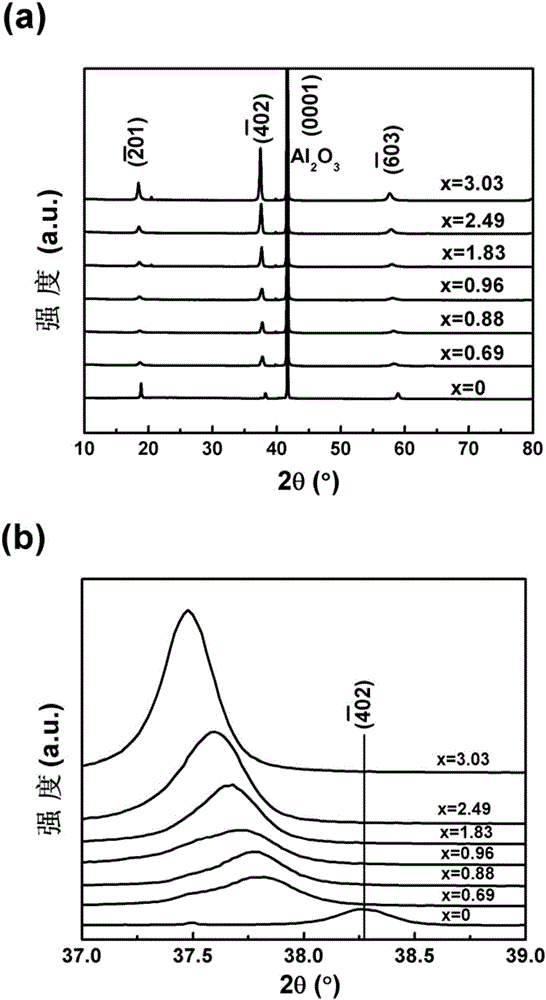
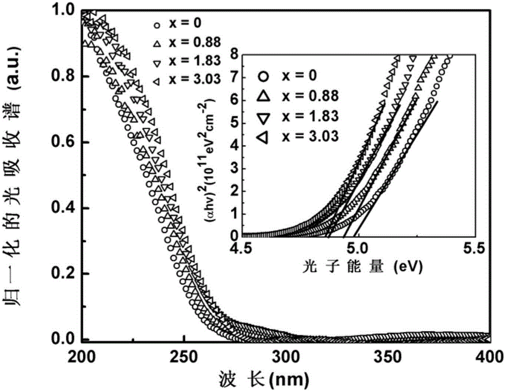
[0026] First take a c-plane sapphire substrate with a size of 10mm×10mm×0.5mm, soak the substrate in acetone, ethanol, and deionized water for 10 minutes, then rinse it with deionized water after taking it out, and finally wash it with dry N 2 Blow dry and set aside. Put the above-mentioned cleaned sapphire substrate into the deposition chamber, and grow a layer of Zn:Ga 2 o 3 thin film, with 99.99% pure Ga 2 o 3 Ceramic as the mother target, in Ga 2 o 3 Different numbers of Zn particles are placed around the glow circle of the target to grow different concentrations of Zn:Ga 2 o 3 Thin films (by XPS for Zn:Ga 2 o 3 Thin film test, Zn:Ga prepared when placing 1, 2, 3, 4, 5, 6 Zn particles 2 o 3 The doping concentration of Zn in the film is respectively 0.69%, 0.88%, 0.96%, 1.83%, 2.49%, 3.03%), and the specific growth parameters of the film...
PUM
| Property | Measurement | Unit |
|---|---|---|
| Thickness | aaaaa | aaaaa |
| Thickness | aaaaa | aaaaa |
| Thickness | aaaaa | aaaaa |
Abstract
Description
Claims
Application Information


