Annealing method for heterojunction solar cell

A solar cell and heterojunction technology, which is applied in circuits, photovoltaic power generation, electrical components, etc., can solve the problems of difficult process, small annealing process interval of heterojunction solar cells, high requirements for sintering process and silver paste, and achieve technological The process is simple, the contact resistance and surface work function are reduced, and the effect of improving battery performance

Inactive Publication Date: 2017-04-26
福建金石能源有限公司
View PDF5 Cites 2 Cited by
  • Summary
  • Abstract
  • Description
  • Claims
  • Application Information

AI Technical Summary

Problems solved by technology

[0005] In view of the above problems, the present invention provides an annealing method for mass-junction solar cells, which uses non-silver metal grid line technology instead of printing silver p

Method used


Image

  • Annealing method for heterojunction solar cell
  • Annealing method for heterojunction solar cell
  • Annealing method for heterojunction solar cell

Examples


Embodiment 1

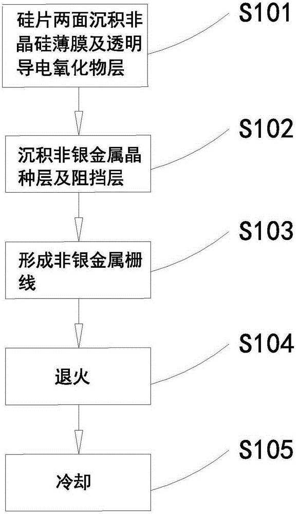
[0035] Such as figure 1 Shown:

[0036] Step S101, depositing a thin intrinsic amorphous silicon layer and an n-type amorphous silicon layer of 10 nm in total on one side of the textured and cleaned n-type silicon substrate, and depositing a thin intrinsic amorphous silicon layer and p A total of 10 nm of non-crystalline silicon layer, and then deposit a transparent conductive oxide ITO thin film of 100 nm on the thin amorphous silicon layer on both sides of the silicon wafer.

[0037] Step S102 , depositing a barrier layer and a 100 nm seed layer by magnetron sputtering on the transparent conductive oxide ITO layer in step S101 .

[0038] Step S103 , forming Cu gate lines on the barrier layer and the seed layer deposited by magnetron sputtering in step S102 by patterning and electrochemical deposition processes.

[0039] Step S104, place the solar cell with the Cu grid lines formed in step S103 in a temperature range of 170°C to 190°C for annealing, the annealing atmosphere...

Embodiment 2

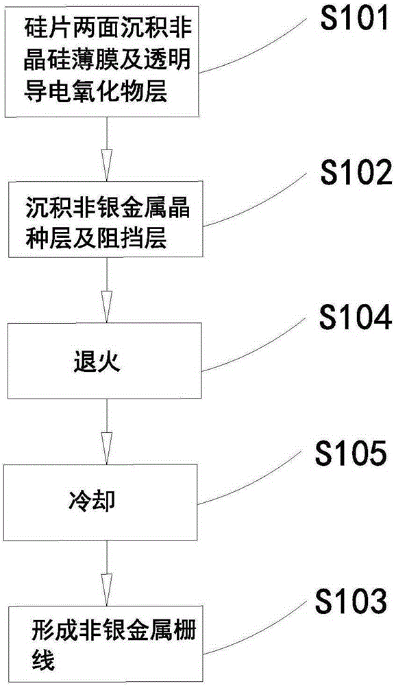
[0042] Such as figure 2 Shown:

[0043] Step S101, depositing a thin intrinsic amorphous silicon layer and a p-type amorphous silicon layer with a total thickness of 10 nm on one side of the p-type silicon substrate having a suede surface after cleaning, and depositing a thin intrinsic amorphous silicon layer and n Type amorphous silicon layer with a total of 10nm, and then deposit a transparent conductive oxide ITO thin film of 90nm on the amorphous silicon thin layer on both sides.

[0044]Step S102 , depositing a barrier layer and a seed layer of 150 nm by magnetron sputtering on the transparent conductive oxide ITO layer.

[0045] Step S104, place the battery semi-finished sheet deposited with the barrier layer and the seed layer at a temperature range of 170°C to 190°C for annealing, the annealing atmosphere is nitrogen, the annealing time is 50 minutes, the annealing pressure is 300 torr, and the whole annealing process is under oxygen The content in the annealing atm...


PUM


Abstract

The invention discloses an annealing method for a heterojunction solar cell. The method comprises: an intrinsic amorphous silicon layer and an n type amorphous silicon layer are deposited on one surface of an n type substrate and an intrinsic amorphous silicon layer and a p type amorphous silicon layer are deposited on the other surface, and a transparent conductive oxide film is deposited on the n type amorphous silicon layer and the p type amorphous silicon layer; a barrier layer and a non-silver metal seed crystal layer are deposited on the transparent conductive oxide layer; and a non-silver metal grid line is deposited on the non-silver metal seed crystal layer. Besides, the method also includes an annealing step: a solar cell is processed by annealing in a temperature range of 120 DEG to 190 DEG, wherein the annealing atmosphere is an atmosphere of non-oxidizing gas; and the solar cell after annealing is cooled. According to the annealing method, the non-silver metal grid line is used for replacing a printed silver line and compatibility with the high-temperature annealing process of the heterojunction cell technology is high, so that the cell performance can be improved; the process becomes simple; the annealing process zone increases; and the annealing condition meets the temperature stability requirement of the amorphous silicon layer.

Description

technical field [0001] The invention relates to the field of solar cell manufacturing, in particular to an annealing method for a heterojunction solar cell. Background technique [0002] The transparent conductive oxide thin film layer in heterojunction solar cell technology is crucial to the performance of heterojunction cells. It needs to have good conductivity to help collect carriers, and as an anti-reflection layer to reduce the reflection of incident light on the surface of the silicon wafer , so that more light can enter the semiconductor light-absorbing layer. After the transparent conductive oxide thin film is deposited into a film, the annealing process can effectively improve the crystallinity of the transparent conductive oxide, and increase the electrical conductivity and light transmittance. Not only that, the intrinsic and doped amorphous silicon layer of the heterojunction cell, and the sputtering deposition process of the transparent conductive oxide film w...

Claims


Application Information

Patent Timeline
IPC IPC(8): H01L31/18H01L31/0224
CPCH01L31/022425H01L31/18H01L31/1864Y02E10/50Y02P70/50
Inventor 黄辉明郭海龙罗骞宋广华陈松洲陈文平
Owner 福建金石能源有限公司
Why Eureka
Try Eureka