High linearity GaN fin-type high electron mobility transistor and manufacture method thereof

A technology with high electron mobility and high linearity, applied in semiconductor/solid-state device manufacturing, circuits, electrical components, etc. Poor performance and other problems, achieve high current drive capability and output power capability, meet the needs of microwave power circuits, and the process method is simple and reliable

Inactive Publication Date: 2017-05-17
NO 55 INST CHINA ELECTRONIC SCI & TECHNOLOGYGROUP CO LTD
View PDF4 Cites 14 Cited by
  • Summary
  • Abstract
  • Description
  • Claims
  • Application Information

AI Technical Summary

Problems solved by technology

However, in order to achieve this goal, the preparation of fins adopts a self-alignment method, the process is complex, and the compatibility with traditional GaN device processes is poor; the most important thing is that the gate electrode of the device prepared by this process is a straight gate structure, and the gate resistance is large. , leading to a low maximum oscillation frequency, which ultimately limits its application in microwave power circuits
[0006] A Chinese patent application discloses a multi-channel fin structure AlGaN / GaN high electron mobility transistor structure and manufacturing method, which mainly solves the problems of poor gate control ability of existing multi-channel devices and low current of FinFET devices
[0007] A Chinese patent application discloses a T-gate N-plane GaN / AlGaN fin-type high electron mobility transistor, which mainly solves the problems of low maximum oscillation frequency, large ohmic contact resistance and serious short channel effect of existing microwave power devices
[0008] Although the above two solutions solve the problems of GaN multi-channel and N-surface structures respectively, there are still obvious deficiencies: the main reason is to adopt the traditional GaN-based fin structure and preparation method, that is, to prepare GaN-based three-dimensional fins first and then prepare concaves. Groove, the three-dimensional fins are not only located in the groove, but also in the area outside the groove, such as "N-face GaN-based fin-type high electron mobility transistor and its manufacturing method" figure 1 shown
Studies have shown that the key to the high linearity of transconductance of the device is that the three-dimensional fins are completely wrapped by the gate metal, and the above two solutions cannot meet this requirement. Therefore, the existing devices do not have high transconductance and high linearity.

Method used


Image

  • High linearity GaN fin-type high electron mobility transistor and manufacture method thereof
  • High linearity GaN fin-type high electron mobility transistor and manufacture method thereof
  • High linearity GaN fin-type high electron mobility transistor and manufacture method thereof

Examples


preparation example Construction

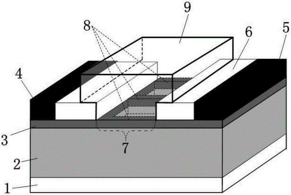
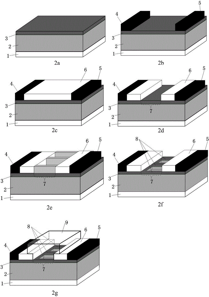
[0039] Reference figure 2 The method for preparing a GaN fin-type high electron mobility transistor with high linearity provided by the present invention includes the following specific steps:

[0040] 1) Grow buffer layer 2 and barrier layer 3 sequentially on substrate 1, such as figure 2 a; Wherein: the material of the substrate 1 is any one of sapphire, SiC, Si, diamond or GaN free-standing substrate; the buffer layer 2 is one or a combination of GaN, AlGaN, AlN, and InGaN; The barrier layer 3 is one or a combination of AlGaN, InAlN, InAlGaN, and AlN.

[0041] 2) Photoetch the source and drain patterns on the barrier layer 3, and deposit the source and drain metals, and then in the N 2 Perform thermal annealing in the atmosphere to fabricate source 4 and drain 5 respectively, such as figure 2 b; wherein: the metal of the source 4 and the drain 5 includes but not limited to Ti / Al, Ti / Au, Ti / Al / W, Ti / Al / Mo / Au, Ti / Al / Ni / Any multi-layer metal of Au, Si / Ti / Al / Ni / Au, Ti / Al / TiN.

[...

Embodiment 1

[0050] Example 1: Preparation of SiC substrate, buffer layer is AlN / GaN, barrier layer is AlGaN, passivation layer is SiN, GaN-based three-dimensional fin width is 100nm, gate metal is Ni / Au / Ni with high linearity The process of a high-degree GaN fin-type high electron mobility transistor is:

[0051] 1) On the SiC substrate 1, using the metal organic chemical vapor deposition technology MOCVD, first grow 100nm AlN at 1050°C, and then grow a 2μm unintentionally doped GaN layer at 1000°C to form the buffer layer 2. Subsequently, an AlGaN barrier layer 3 with a thickness of 22 nm is grown on the buffer layer 2 with an Al composition of 30%.

[0052] 2) Make a photolithography mask on the barrier layer 3, then use electron beam evaporation to deposit the metal stack, and obtain isolated metal blocks at both ends of the stripping process, and finally 2 The source 4 and the drain 5 are formed by rapid thermal annealing in an atmosphere. The deposited metals are Ti, Al, Ni and Au from b...

Embodiment 2

[0060] Example 2: Preparation of Si substrate, buffer layer is AlN / AlGaN / GaN layer, barrier layer is AlN / InAlN, passivation layer is SiO 2 The GaN-based three-dimensional fin width is 400nm, and the gate metal is TiN / Ti / Al / Ti / TiN GaN fin-type high electron mobility transistor with high linearity. The process is:

[0061] 1) On the Si substrate, using the metal organic chemical vapor deposition technology MOCVD, first grow 200nm AlN at 1050℃, and then grow a 1μm unintentionally doped AlGaN layer (Al group 15%) and A 500nm GaN layer is formed to form the buffer layer 2, and then an AlN layer with a thickness of 1 nm and 8nm InAlN are grown on the buffer layer 2 at 800°C to form a barrier layer 3 with an Al composition of 83%.

[0062] 2) Make a photolithography mask on the barrier layer 3, then use electron beam evaporation to deposit the metal stack, and obtain isolated metal blocks at both ends of the stripping process, and finally 2 The source electrode 4 and the drain electrode 5 ...


PUM


Abstract

The present invention relates to a high linearity GaN fin-type high electron mobility transistor and a manufacture method thereof. From bottom to top, the transistor sequentially comprises a substrate, a buffer layer, a barrier layer, and a passivation layer. A source electrode is arranged at one end above the barrier layer and a drain electrode is arranged at the other end. The passivation layer is arranged above the barrier layer between the source electrode and the drain electrode. A groove is arranged in the passivation layer. A T-shaped gate is arranged in the groove. The transistor is characterized in that GaN-based three-dimensional fins in periodical arrangement are etched only on the barrier layer and the buffer layer in an area below the groove, the length of the GaN-based three-dimensional fins is equal to the length of the groove, and an isolation groove that is etched is arranged between adjacent GaN-based three-dimensional fins. The transistor has high linearity and output current, strong gate control capability, good heat dissipation performance, and high frequency characteristic. The manufacture method is simple and reliable, and is applicable to high power, high linearity microwave power devices.

Description

Technical field [0001] The invention belongs to the technical field of semiconductor device preparation, and particularly relates to a GaN fin type high electron mobility transistor with high linearity and a manufacturing method thereof. [0002] technical background [0003] The third-generation semiconductor GaN-based High Electron Mobility Transistor (HEMT) has the characteristics of high output power density, high efficiency, high temperature resistance, and radiation resistance. It has become the mainstream technology for manufacturing high-frequency, high-efficiency, high-power electronic devices. Improved the performance of weapons and equipment represented by radar. With the urgent demand for high-linearity transistors in high-data-flow satellite communications and modern wireless communication applications (such as 5G communications), high-linearity devices have now become a key development direction in the GaN field. High linearity will bring more effective spectrum util...

Claims


Application Information

Patent Timeline
Patent Type & Authority Applications(China)
IPC IPC(8): H01L29/778H01L29/06H01L29/423H01L21/336
Inventor 张凯孔月婵周建军陈堂胜
Owner NO 55 INST CHINA ELECTRONIC SCI & TECHNOLOGYGROUP CO LTD
Why Eureka
Try Eureka