High linearity millimeter-wave device and manufacturing method thereof

A high-linearity, millimeter-wave technology, applied in the field of microelectronics, can solve the problems of increased influence of frequency characteristics of parasitic capacitor devices, decreased gate control ability, and poor gate support, so as to improve frequency characteristics, improve linearity, Effect of reducing square resistance and contact resistance

Active Publication Date: 2019-08-13
XIDIAN UNIV
View PDF4 Cites 0 Cited by
  • Summary
  • Abstract
  • Description
  • Claims
  • Application Information

AI Technical Summary

Problems solved by technology

[0008] First, when the gate length of the device is less than 100nm, reducing the gate width will lead to poor support of the gate;
[0009] Second, as the gate-to-drain spacing decreases, the influence of parasitic capacitance on the frequency characteristics of the device will increase;
[0010] The third is that as the gate width decreases, the gate control capability decreases, resulting in a decrease in the linearity of the transconductance

Method used


Image

  • High linearity millimeter-wave device and manufacturing method thereof
  • High linearity millimeter-wave device and manufacturing method thereof

Examples


Embodiment 1

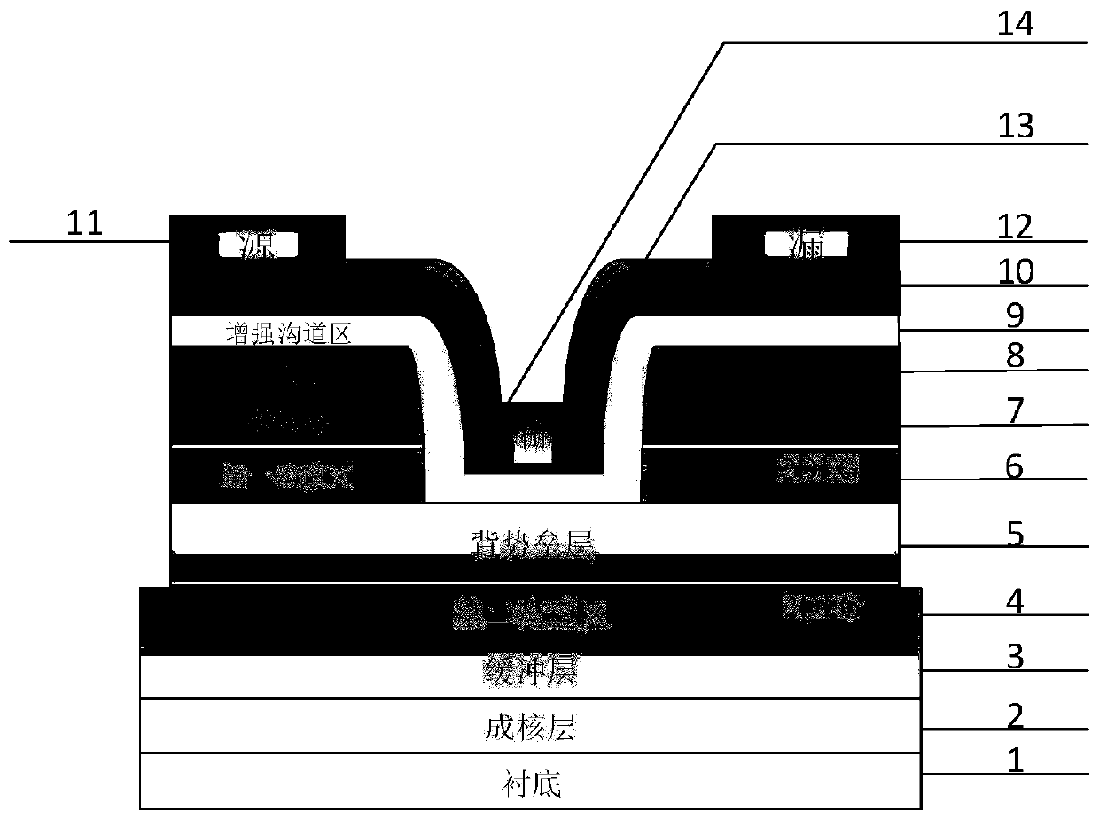
[0037] Embodiment 1: On a sapphire substrate, the groove width is 0.2 μm, the groove etching depth is 35 nm, the barrier layer is an AlGaN layer with a thickness of 3 nm, the thickness of the enhanced channel region is 2 nm, and the thickness of the conductive cap layer is 10nm high linearity millimeter wave device.

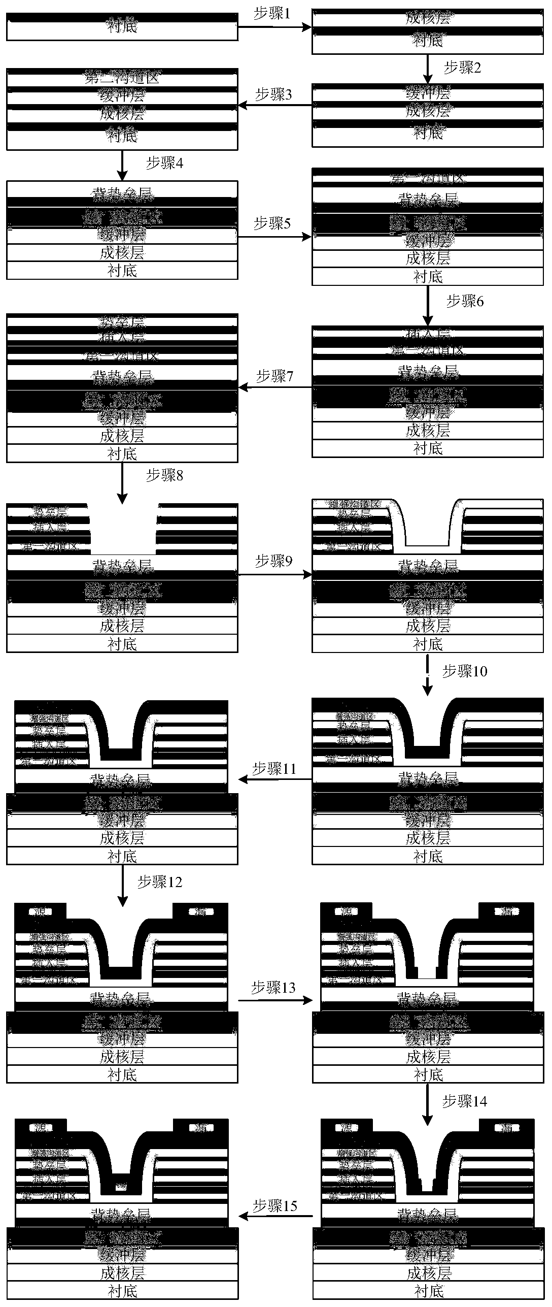
[0038] In step 1, an AlN nucleation layer is grown on a sapphire substrate by MOCVD process.

[0039] First lower the temperature of the sapphire substrate to 500°C, keep the growth pressure at 40Torr, the flow rate of hydrogen gas at 1000sccm, the flow rate of ammonia gas at 600sccm, feed the aluminum source with a flow rate of 4sccm into the reaction chamber, and grow a sapphire substrate with a thickness of 5nm. Low temperature AlN layer;

[0040]Then increase the growth temperature to 940°C, keep the growth pressure at 40 Torr, the flow rate of hydrogen gas at 1000 sccm, the flow rate of ammonia gas at 1000 sccm, feed the aluminum source with a flow rate of ...

Embodiment 2

[0113] Embodiment 2, the groove width is 1 μm on the SiC substrate, the groove etching depth is 120nm, the barrier layer is an AlGaN layer with a thickness of 50nm, the thickness of the enhanced channel region is 10nm, and the thickness of the conductive cap layer is 30nm high linearity millimeter wave device.

[0114] In step 1, an AlN nucleation layer is grown on the SiC substrate by using the MOCVD process.

[0115] First lower the temperature of the SiC substrate to 650°C, keep the growth pressure at 100Torr, the flow rate of hydrogen gas at 5000 sccm, the flow rate of ammonia gas at 3000 sccm, and feed the aluminum source with a flow rate of 20 sccm into the reaction chamber to grow a 10nm-thick film on the SiC substrate. Low temperature AlN layer;

[0116] Then increase the growth temperature to 1050°C, keep the growth pressure at 100 Torr, the flow rate of hydrogen gas at 5000 sccm, the flow rate of ammonia gas at 3000 sccm, feed the aluminum source with a flow rate of...

Embodiment 3

[0160] Embodiment 3, on the sapphire substrate, the groove width is 0.2 μm, the groove etching depth is 35nm, the barrier layer is an InAlN layer, the thickness is 3nm, the thickness of the enhanced channel region is 2nm, and the thickness of the conductive cap layer is 10nm high linearity millimeter wave device.

[0161] In step A, an AlN nucleation layer is grown on the sapphire substrate by MOCVD process.

[0162] The specific implementation of this step is the same as step 1 in the first embodiment.

[0163] Step B, growing a GaN buffer layer on the AlN nucleation layer.

[0164] The specific implementation of this step is the same as step 2 in the first embodiment.

[0165] Step C, growing a second channel region on the buffer layer.

[0166] The specific implementation of this step is the same as step 3 in the first embodiment.

[0167] Step D, growing a back barrier layer on the second channel region.

[0168] The specific implementation of this step is the same as...


PUM


Abstract

The invention discloses a high-linearity millimeter wave device and a making method thereof mainly in order to solve the problem that the existing device is of poor linearity of trans-conductance. The device comprises, from bottom to top, a substrate layer (1), a nucleation layer (2), a buffer layer (3), a second channel region (4), a back barrier layer (5), a first channel region (6), an insertion layer (7), and a barrier layer (8). A groove reaching the back barrier layer is formed in the barrier layer through etching. An enhanced channel region (9) is arranged on the inside wall of the groove and on the barrier layer. A conductive cap layer (10) is arranged on the enhanced channel region. A source electrode (11) and a drain electrode (12) are arranged at the two ends of the conductive cap layer. A grooved gate is engraved on the conductive cap layer in the groove. A passivation layer (13) is arranged on the inside wall of the grooved gate and on the conductive cap layer other than the source electrode and the drain electrode. A T-shaped gate electrode (14) is arranged on the passivation layer in the grooved gate. The trans-conductance peak range is widened, and the linearity of trans-conductance is increased. The high-linearity millimeter wave device can be used in communication, navigation, radar, and base station systems.

Description

technical field [0001] The invention belongs to the technical field of microelectronics, and in particular relates to a high linearity millimeter wave device, which can be used in communication, satellite navigation, radar system and base station system. Background technique [0002] With the improvement of technology level, the existing first and second generation semiconductor materials can no longer meet the needs of higher frequency and higher power electronic devices, while electronic devices based on nitride semiconductor materials can meet this requirement, greatly improving The improvement of device performance has made the third-generation semiconductor materials represented by GaN widely used in the manufacture of microwave and millimeter wave devices. GaN is a new type of wide bandgap compound semiconductor material, which has excellent characteristics that many silicon-based semiconductor materials do not have, such as wide bandgap width, high breakdown electric ...

Claims


Application Information

Patent Timeline
Patent Type & Authority Patents(China)
IPC IPC(8): H01L29/06H01L21/336
CPCH01L29/0642H01L29/0688H01L29/66409
Inventor 杨凌康慨周小伟马晓华郝跃
Owner XIDIAN UNIV
Why Eureka
Try Eureka