P-type PERC solar energy cell preparation method, cell, assembly and system

A solar cell, N-type technology, applied in the field of solar cells, can solve the problems of scratches on silicon wafers, increase the fragmentation rate, etc., and achieve the effects of increasing the breakage rate, reducing the fragmentation rate, and improving the conversion efficiency of cells

Inactive Publication Date: 2017-08-18
GUANGDONG AIKO SOLAR ENERGY TECH CO LTD
View PDF5 Cites 15 Cited by
  • Summary
  • Abstract
  • Description
  • Claims
  • Application Information

AI Technical Summary

Problems solved by technology

However, the silicon nitride film on the front side, the silicon nitride film on the back side, and the aluminum oxide film on the back side all need to be deposited successively. Multiple operations and steps are likely to cause scratches on the silicon wafer and increase the fragmentation rate, which is not conducive to reducing the defective rate of the product.

Method used


Image

  • P-type PERC solar energy cell preparation method, cell, assembly and system
  • P-type PERC solar energy cell preparation method, cell, assembly and system
  • P-type PERC solar energy cell preparation method, cell, assembly and system

Examples


preparation example Construction

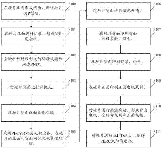
[0039] Such as figure 1 Shown, the present invention provides a kind of preparation method of P-type PERC solar cell, comprises the following steps:

[0040] S100, forming a textured surface on the front side of the silicon wafer, where the silicon wafer is P-type silicon.

[0041] Use wet or dry etching technology to form a textured surface on the surface of the silicon wafer through texturing equipment.

[0042] S101, performing diffusion on the front side of the silicon wafer to form an N-type emitter.

[0043] The diffusion in step S101 of the preparation method of the present invention is to place the silicon wafer in a thermal diffusion furnace for diffusion, and form an N-type emitter above the P-type silicon. During the diffusion, the temperature should be controlled within the range of 800°C-900°C. The target square resistance is 90-150 ohm / □.

[0044] During the diffusion process, a phosphosilicate glass layer will be formed on the front and back of the silicon wa...

Embodiment 1

[0070] (1) Form a textured surface on the front of the silicon wafer by wet texturing, and the silicon wafer is P-type silicon.

[0071] (2) Place the silicon wafer in a thermal diffusion furnace for diffusion, and form an N-type emitter above the P-type silicon. During diffusion, the temperature should be controlled within the range of 840°C, and the target sheet resistance is 90Ω / □.

[0072] (3) Place the diffused silicon wafer in HF and HNO with a volume ratio of 1:5 3 Soak in the mixed solution acid tank for 15s to remove the phosphosilicate glass and surrounding PN junctions.

[0073] (4) Deposit an aluminum oxide film on the back of the silicon wafer using conventional PECVD equipment.

[0074] (5) Use PECVD double-sided deposition equipment to deposit silicon nitride film on the front and back of the silicon wafer at the same time. Among them, the rate of silane gas ejected downward from the vent plate on the process chamber is 1600 sccm, and the rate of ammonia gas is...

Embodiment 2

[0082] (1) Form a textured surface on the front of the silicon wafer by wet texturing, and the silicon wafer is P-type silicon.

[0083] (2) Place the silicon wafer in a thermal diffusion furnace for diffusion, and form an N-type emitter above the P-type silicon. During diffusion, the temperature should be controlled within the range of 830°C, and the target sheet resistance is 100Ω / □.

[0084] (3) Place the diffused silicon wafer in HF and HNO with a volume ratio of 1:5 3 Soak in the mixed solution acid tank for 15s to remove the phosphosilicate glass and surrounding PN junctions.

[0085] (4) Deposit an aluminum oxide film on the back of the silicon wafer using conventional PECVD equipment.

[0086] (5) Use PECVD double-sided deposition equipment to deposit silicon nitride film on the front and back of the silicon wafer at the same time. Among them, the rate of silane gas ejected downward from the vent plate on the process chamber is 1650 sccm, and the rate of ammonia gas i...


PUM

PropertyMeasurementUnit
thicknessaaaaaaaaaa
thicknessaaaaaaaaaa
thicknessaaaaaaaaaa

Abstract

The invention discloses a P-type PERC solar energy cell preparation method. The P-type PERC solar energy cell preparation method comprises steps that (1), a suede-like surface is formed at a front surface of a silicon chip; (2), diffusion is carried out at the front surface of the silicon chip, and an N-type emitter electrode is formed; (3), phosphorosilicate glass and peripheral PN junctions are removed; (4), an alumina film is deposited at a back surface of the silicon chip; (5), PECVD double-surface deposition equipment is employed, and silicon nitride films are deposited at the front surface and the back surface of the silicon chip; (6), laser grooving at the back surface of the silicon chip is carried out; (7), back surface electrode slurry is printed at the back surface of the silicon chip and is then dried; (8), aluminum slurry is printed at the back surface of the silicon chip and is then dried; (9), front surface electrode slurry is printed at the front surface of the silicon chip; (10); high temperature sintering is carried out for the silicon chip, and a back surface electrode, a full aluminum back electric field and a front surface electrode are formed; and (11), anti-LID annealing for the silicon chip is carried out, and the P-type PERC solar energy cell is acquired. The invention further discloses the P-type PERC solar energy cell, an assembly and a system. The method is advantaged in that production efficiency can be improved, and scratch of the silicon chip is reduced.

Description

technical field [0001] The present invention relates to the technical field of solar cells, and in particular to a method for preparing a P-type PERC solar cell. Correspondingly, the present invention also relates to a P-type PERC solar cell, a component and a system. Background technique [0002] Crystalline silicon solar cell is a device that effectively absorbs solar radiation energy and converts light energy into electrical energy by using the photovoltaic effect. Under the action, holes flow from the N region to the P region, electrons flow from the P region to the N region, and a current is formed after the circuit is turned on. [0003] Traditional crystalline silicon solar cells basically only use front passivation technology, depositing a layer of silicon nitride film on the front surface of the silicon wafer by PECVD to reduce the recombination rate of minority carriers on the front surface, which can greatly increase the open circuit voltage and Short-circuit cur...

Claims


Application Information

Patent Timeline
Patent Type & Authority Applications(China)
IPC IPC(8): H01L31/048H01L31/18
CPCH01L31/048H01L31/049H01L31/18Y02E10/50Y02P70/50
Inventor 何达能方结彬陈刚
Owner GUANGDONG AIKO SOLAR ENERGY TECH CO LTD
Why Eureka
Try Eureka