Gallium nitride base film on flexible polyimide substrate and preparing method of gallium nitride base film

A technology based on polyimide and gallium nitride, which is applied in the direction of gaseous chemical plating, semiconductor/solid-state device manufacturing, coating, etc., and can solve the problems of not being able to block the diffusion of water and oxygen

Active Publication Date: 2017-08-22
DALIAN UNIV OF TECH
View PDF6 Cites 13 Cited by
  • Summary
  • Abstract
  • Description
  • Claims
  • Application Information

AI Technical Summary

Problems solved by technology

[0004] However, at present, metal organic chemical vapor deposition (MOCVD) method is mainly used in industry to grow Al x Ga y In 1-x-y The growth of N thin films and devices usually requires a high temperature of about 1050°C, while the temperature resistance of polyimide substrates generally does not exceed 550°C, so the preparation of Al on polyimide substrates x Ga y In 1-x-y N thin films require a low-temperature growth method. On the other hand, polyimide cannot block the diffusion of water and oxygen, and polyimide is a non-single crystal substrate, so it is difficult to directly grow Al with high crystal quality. x Ga y In 1-x-y N thin films are therefore required on polyimide substrates with Al x Ga y In 1-x-y A suitable water and oxygen barrier layer and an intermediate layer material for epitaxy are inserted between the N films

Method used


Image

  • Gallium nitride base film on flexible polyimide substrate and preparing method of gallium nitride base film
  • Gallium nitride base film on flexible polyimide substrate and preparing method of gallium nitride base film
  • Gallium nitride base film on flexible polyimide substrate and preparing method of gallium nitride base film

Examples


Embodiment Construction

[0041] The specific embodiments of the present invention will be further described below with reference to the drawings and technical solutions.

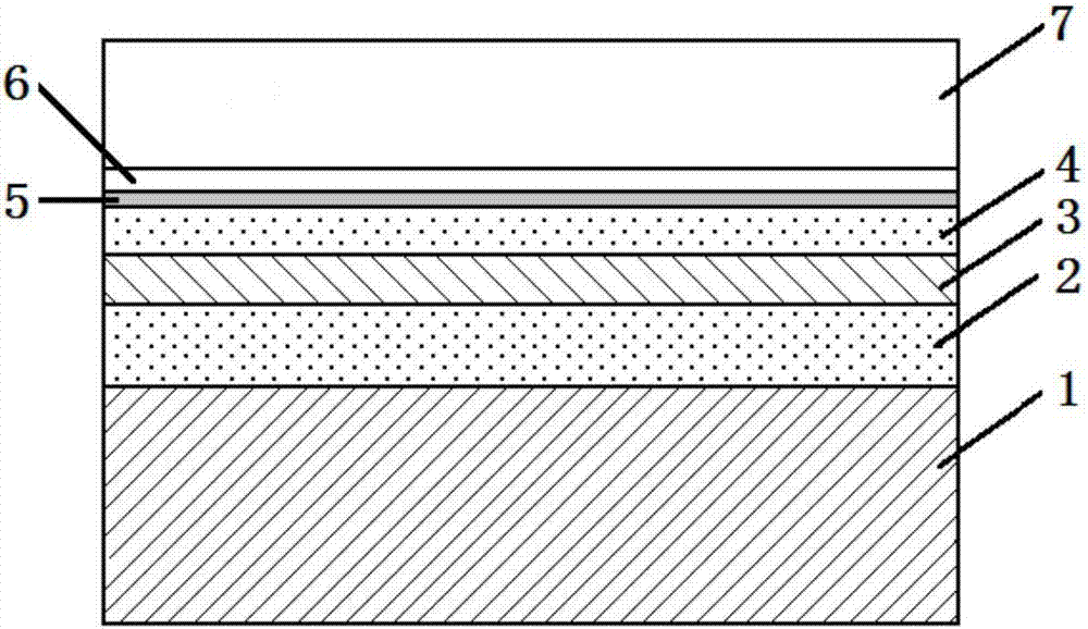
[0042] One of the embodiments, as attached figure 1 , 2 and 3.

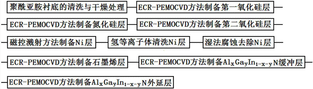
[0043] One uses magnetron sputtering equipment and ECR-PEMOCVD equipment (invention patent: ZL201210247144.8), prepared at low temperature on polyimide substrate 1, as attached figure 1 Al shown 0.10 Ga 0.40 In 0.50 The continuous process steps of N film are:

[0044] a. ECR-PEMOCVD method to prepare the first silicon oxide layer 2: Use absorbent cotton balls soaked in absolute ethanol to wipe the surface of the polyimide substrate 3 times in one direction, and then place the polyimide substrate 1 in order. Ultrasonic cleaning in water ethanol and deionized water 3 times each for 5 minutes, and then place the polyimide substrate 1 on a hot plate at 120°C for 10 minutes; the dried polyimide substrate 1 Put it into the glove box of the ECR-PEMOCVD equipment, and then transfer ...


PUM

PropertyMeasurementUnit
thicknessaaaaaaaaaa
thicknessaaaaaaaaaa
thicknessaaaaaaaaaa

Abstract

The invention belongs to the field of III group nitride film and device manufacturing, and provides a gallium nitride base film on a flexible polyimide substrate and a preparing method of the gallium nitride base film. Specifically, polyimide serves as the substrate, a first silicon oxide layer, a silicon nitride layer and a second silicon oxide layer are sequentially prepared on the polyimide substrate through an ECR-PEMOCVD method, then a Ni layer is prepared on the second silicon oxide layer through a magnetron sputtering method, a graphene layer is prepared on the interface of the Ni layer and the second silicon oxide layer through the ECR-PEMOCVD method, then, the Ni layer is removed through a wet etching method, and finally, an AlxGayIn1-x-yN buffering layer and an epitaxial layer are sequentially prepared on the graphene layer through the ECR-PEMOCVD method. A prepared AlxGayIn1-x-yN film can be used for preparing InGaN solar cells, AlGaN ultraviolet detectors, GaN film thin film transistors and other flexible devices.

Description

Technical field [0001] The present invention belongs to the field of III-nitride film and device manufacturing, and particularly relates to a gallium nitride-based film on a polyimide substrate and a preparation method thereof. Specifically, the polyimide (PI) is used as the substrate. Electron cyclotron resonance-plasma-enhanced metal organic chemical vapor deposition (ECR-PEMOCVD) method is used to prepare the first silicon oxide layer, the silicon nitride layer, and the second silicon dioxide layer on the polyimide substrate, and then use the magnetron Sputtering method prepares Ni layer on the second silicon dioxide layer, then uses ECR-PEMOCVD method to prepare graphene layer on the interface between Ni layer and the second silicon dioxide layer, then uses wet etching method to remove Ni layer, and finally uses ECR -PEMOCVD method sequentially prepares Al on the graphene layer x Ga y In 1-x-y N buffer layer and Al x Ga y In 1-x-y N epitaxial layer. Background technique [0...

Claims


Application Information

Patent Timeline
Patent Type & Authority Applications(China)
IPC IPC(8): C23C16/34C23C16/40C23C16/26H01L21/02
CPCC23C16/26C23C16/303C23C16/345C23C16/402H01L21/02422H01L21/02458H01L21/0254H01L21/0262
Inventor 秦福文马春雨白亦真王德君林国强
Owner DALIAN UNIV OF TECH
Why Eureka
Try Eureka