A High-Sensitivity Broadband Optical Receiver Front-End Circuit

A receiver front-end, high-sensitivity technology, applied in electromagnetic receivers, electrical components, electromagnetic wave transmission systems, etc., can solve problems such as difficult to achieve high-sensitivity broadband optical receivers, achieve good application prospects, enhance functions, improve circuits The effect of sensitivity

Inactive Publication Date: 2019-06-14
TIANJIN UNIV
View PDF5 Cites 1 Cited by
  • Summary
  • Abstract
  • Description
  • Claims
  • Application Information

AI Technical Summary

Problems solved by technology

[0005] However, due to the indirect bandgap characteristics of the silicon material itself and the limitations of the process structure, as well as the influence of the detector input capacitance on the bandwidth and noise characteristics of the entire circuit, it is difficult to achieve a high-sensitivity broadband optical receiver

Method used


Image

  • A High-Sensitivity Broadband Optical Receiver Front-End Circuit
  • A High-Sensitivity Broadband Optical Receiver Front-End Circuit
  • A High-Sensitivity Broadband Optical Receiver Front-End Circuit

Examples


Embodiment 1

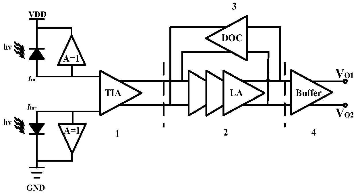
[0047] A high-sensitivity broadband optical receiver front-end circuit, see figure 1 , the broadband optical receiver front-end circuit includes:

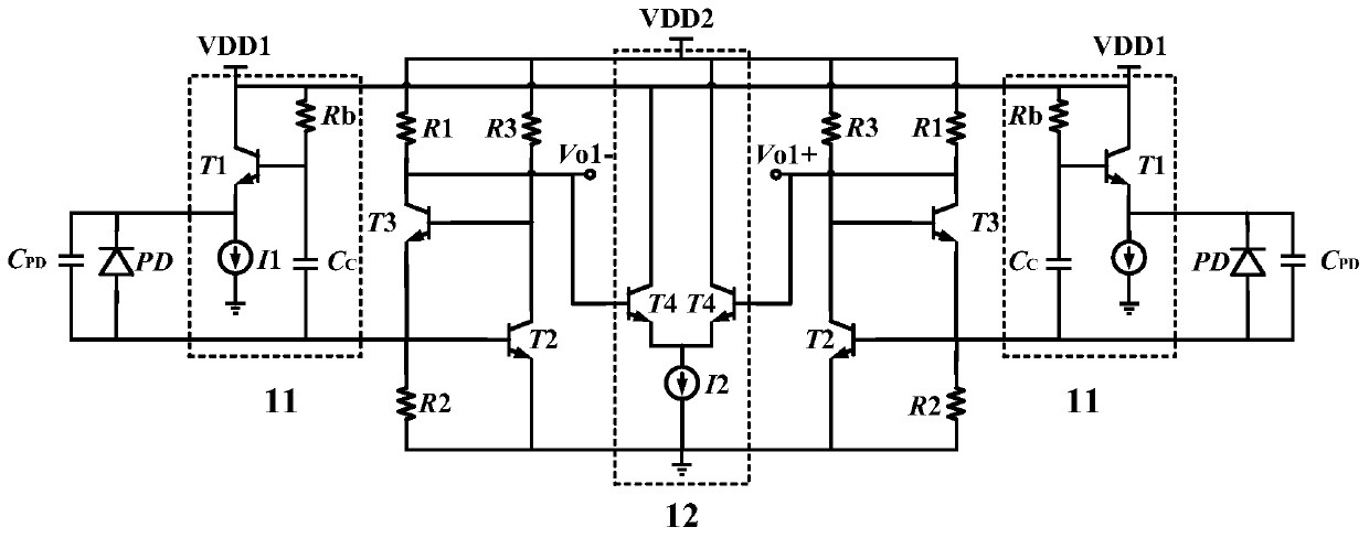
[0048] 1. A bootstrap circuit 11 is added to the input of the transimpedance amplifier 1 to reduce the influence of the detector capacitance on the subsequent circuit;

[0049] 2. A noise elimination circuit 12 is added to the transimpedance amplifier 1 to reduce the noise caused by the change of the power supply current and improve the sensitivity of the circuit;

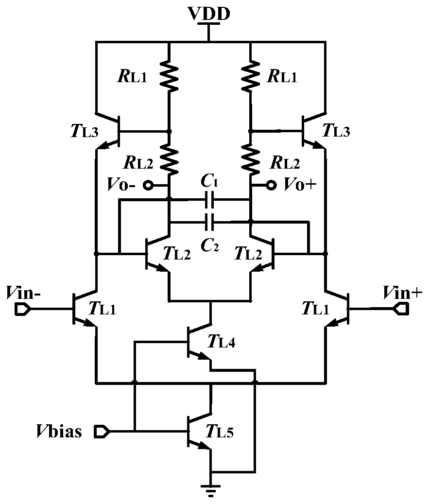
[0050] 3. The limiting amplifier 2 adopts a Cherry-Hooper structure with negative Miller compensation, which is used to amplify the voltage signal output by the transimpedance amplifier 1 to the voltage level required by the digital processing unit;

[0051]4. The DC offset elimination circuit 3 using differential active Miller capacitors is used to eliminate the influence of DC offset on the circuit;

[0052] 5. In order to achieve output impedance matching and provi...

Embodiment 2

[0055] Combine below Figure 2-Figure 6 , and the specific calculation formula further introduces the scheme in embodiment 1, see the following description for details:

[0056] The embodiment of the invention provides a high-sensitivity broadband optical receiver front-end circuit. The front-end circuit of the receiver fully utilizes the advantages of high-speed and strong driving capability of bipolar circuits of germanium-silicon heterojunction and low power consumption and high integration of CMOS circuits. The schematic diagram of the circuit structure of the optical receiver designed in the embodiment of the present invention is as follows figure 1 shown. The front-end circuit of the optical receiver includes: a transimpedance amplifier 1 with a bootstrap circuit and a noise elimination circuit, a group of three-stage cascaded limiting amplifiers with negative Miller capacitance compensation 2, a DC using differential active Miller capacitance Offset cancellation circ...


PUM


Abstract

The invention discloses a high-sensitivity broadband optical receiver front-end circuit. The optical receiver front-end circuit comprises a transimpedance amplifier, a limiting amplifier, a DC offset cancellation circuit and an output buffer stage that are sequentially and electrically connected, wherein a bootstrap circuit is additionally arranged at the input end of the transimpedance amplifier to reduce the influence of the detector capacitance; the transimpedance amplifier is provided with a noise elimination circuit to reduce noises caused by the change of power supply current and improve the sensitivity; the limiting amplifier is a set of three-stage cascades, has negative Miller capacitor compensation, and is used for amplifying a voltage signal to the voltage level required by a digital processing unit; the DC offset cancellation circuit adopts a differential active Miller capacitor circuit to eliminate the effects of DC offsets; and the output buffer stage adopts an Ft frequency multiplier structure. According to the high-sensitivity broadband optical receiver front-end circuit disclosed by the invention, the limitation of an input capacitor on a working band of an RGC input stage can be counteracted by using the bootstrap circuit, the noises of the power supply current can be reduced by using the noise elimination circuit, and thus the sensitivity of the circuit can be improved.

Description

technical field [0001] The present invention relates to the field of optical communication, optical interconnection and visible light communication system, in particular to a high-sensitivity sensor compatible with silicon-germanium bipolar-complementary metal-oxide-semiconductor (SiGe BiCMOS) process, designed with bootstrap circuit and noise elimination technology Broadband optical receiver front-end circuit. Background technique [0002] With the continuous improvement of social informatization, broadband services represented by ultra-high-definition video, cloud computing, and mobile Internet are booming, which has doubled the demand for network bandwidth and data traffic in human society. In order to meet the transmission of massive information, breakthroughs have been made in ultra-high-speed, ultra-large-capacity optical fiber communication technology for trunk network transmission. However, limited by technology and cost, the "last mile" of optical fiber communicati...

Claims


Application Information

Patent Timeline
Patent Type & Authority Patents(China)
IPC IPC(8): H04B10/69
CPCH04B10/693H04B10/6931H04B10/6932H04B10/6933H04B10/697H04B10/6972
Inventor 谢生谷由之毛陆虹
Owner TIANJIN UNIV
Why Eureka
Try Eureka