

Method for transferring and preparing two-dimensional atomic crystal laminated structure
A two-dimensional atomic crystal, stacked structure technology, applied in semiconductor/solid-state device manufacturing, electrical components, circuits, etc., can solve the problems of bubble generation, small sample area, easy sample breakage, etc., to reduce doping and damage, The effect of high separation repetition rate and easy residual glue disposal
- Summary
- Abstract
- Description
- Claims
- Application Information
AI Technical Summary
Problems solved by technology
Method used
Image

Examples
Embodiment 1
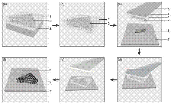
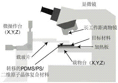
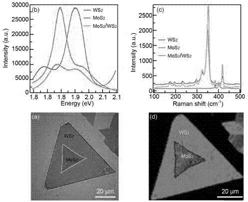
[0038] Positional transfer technology is suitable for the preparation of stacked structures (homojunction and heterojunction) of CVD-grown two-dimensional nanomaterials, so that tungsten disulfide (WS) grown on sapphire substrates 2 / Sapphire) localized molybdenum disulfide (MoS2) transferred to a silicon dioxide substrate 2 / SiO 2 ), so as to prepare a two-dimensional atomic crystal heterojunction as an example, which specifically includes the following steps:
[0039] (1) Toluene was used as a solvent to prepare a polystyrene (PS) solution, and the PS was dissolved by heating with magnetic stirring.
[0040] (2) Prepare dimethylsiloxane (PDMS), mix the main agent (A glue) and the hardener (B glue), remove the air bubbles in the mixed glue by centrifugation, pour it into the container, control the thickness to about 1 mm, and bake curing;
[0041] (3) subbed, in WS 2 / Sapphire surface is spin-coated with PS solution and heated for 30 minutes, then dried toluene solvent; ...
Embodiment 2
[0049] The experimental method is the same as in Example 1, and the single-layer MoS 2 Replaced by single-layer WS 2 , two layers of WS prepared by positioning transfer 2 homogeneous junction.
Embodiment 3
[0051] The experimental method is the same as in Example 1, the only difference is that the monolayer molybdenum disulfide is replaced by molybdenum trioxide nanosheets, and the WS prepared by positioning transfer 2 / MoO 3 Heterojunction.
PUM
| Property | Measurement | Unit |
|---|---|---|
| Thickness | aaaaa | aaaaa |
Abstract
Description
Claims
Application Information