

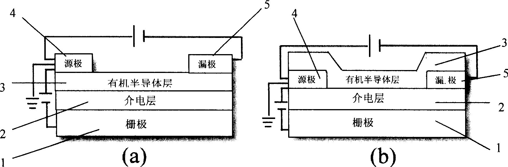
Organic field effect transistor and special source/drain electrode and preparation method thereof
An organic field and electrode technology, which is applied in the field of patterned graphene electrodes and preparation, can solve problems such as difficult graphene patterning, and achieve the effects of improved performance, good contact, and easy large-scale preparation
- Summary
- Abstract
- Description
- Claims
- Application Information
AI Technical Summary
Problems solved by technology
Method used
Image

Examples
preparation example Construction
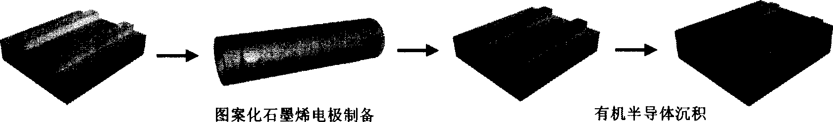
[0035] 1) Preparation of patterned metal thin film:
[0036] The substrate deposited with the gate electrode and the insulating layer is ultrasonically cleaned with deionized water, ethanol, and acetone, and then dried in an oven, and then at least one layer of metal film is prepared, and its patterning is realized through a mask plate or photolithography technology.
[0037] 2) Preparation of patterned graphene source-drain electrodes:
[0038] The substrate with the patterned metal film is placed in a chemical vapor deposition system, and graphene is chemically vapor deposited on the surface of the patterned metal film to obtain a patterned graphene electrode, which is used as the source and drain electrodes of the organic field effect transistor.
[0039] The third step, the deposition of organic semiconductor materials:
[0040]An organic semiconductor layer with a thickness of 10-150 nanometers is prepared on the substrate with the graphene source-drain electrodes and th...
Embodiment 1
[0046] The following example illustrates the preparation of a pentacene-based organic field-effect transistor whose electrode is a graphene-modified copper electrode, but the present invention is not limited thereto.
[0047] The first step is to sequentially deposit gate electrodes and dielectric layers on the substrate according to conventional methods;
[0048] Highly doped N-type single crystal silicon is selected as the substrate and gate electrode, and a silicon dioxide dielectric layer is grown by thermal oxidation.
[0049] The second step is to prepare patterned graphene source and drain electrodes
[0050] 1. Deposition of patterned copper film:
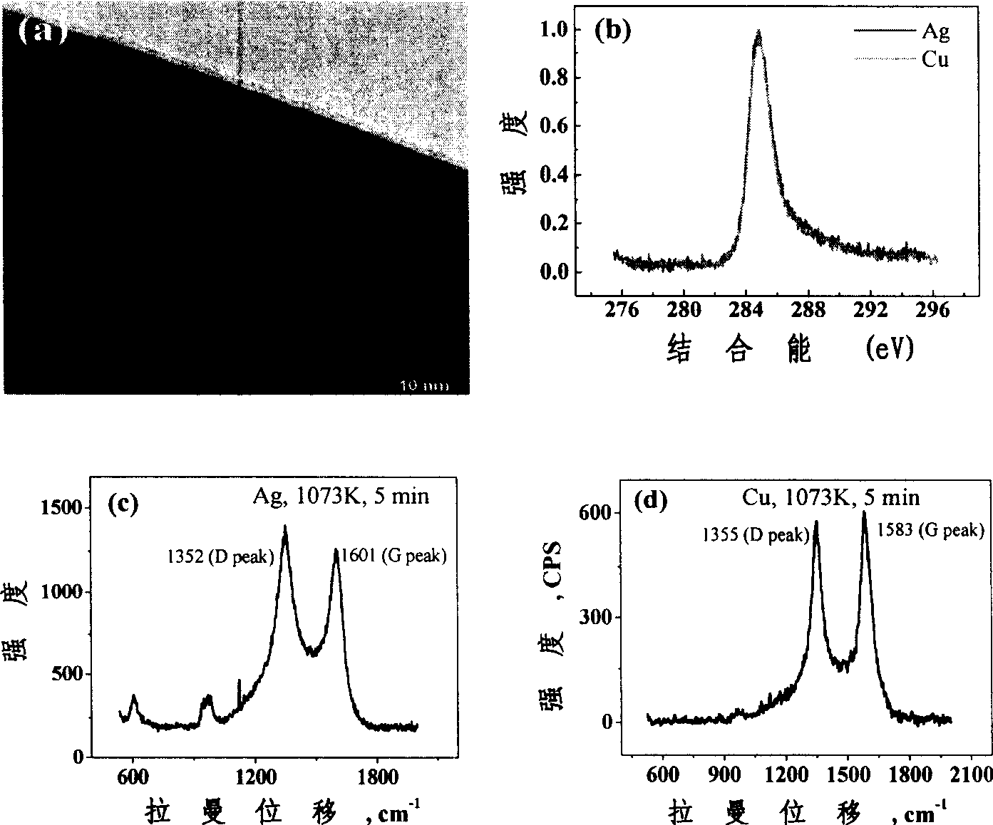
[0051] Such as figure 2 , the substrate deposited with the gate electrode and insulating layer was ultrasonically cleaned with deionized water, ethanol and acetone, and then dried in an oven, and then a 30-nanometer thick copper layer was prepared by plasma-enhanced vacuum thermal evaporation deposition method; The inte...
Embodiment 2
[0061] According to the preparation of Example 1, photolithography was used to prepare interdigitated thin films to realize the patterning of the silver thin film; then, a graphene thin film was grown on the silver thin film as the source and drain electrodes; the remaining steps were the same as in Example 1.
[0062] The performance test of the transistor shows that the pentacene-based crystal has a field effect mobility of 0.48cm when the channel length is 5 microns 2 V -1 the s -1 , an on-off ratio of 10 7 . As a comparison, the mobility of an organic field effect transistor with a lower electrode structure directly using silver electrodes as source and drain electrodes can reach 0.026cm 2 V -1 the s -1 , an on-off ratio of 10 4 . The results show that the organic field effect transistor with graphene as the source and drain electrodes is superior to the device with silver as the electrode in performance, that is to say: compared with silver, the graphene electrode ...
PUM
| Property | Measurement | Unit |
|---|---|---|
| thickness | aaaaa | aaaaa |
Abstract
Description
Claims
Application Information