A kind of preparation method of ultra-thin film and organic field effect transistor sensor based on it

A gas sensor and transistor technology, which is used in instruments, scientific instruments, measuring devices, etc., to achieve the effects of low requirements for equipment and process conditions, simple operation and wide selection.

Active Publication Date: 2019-08-30
HEFEI UNIV OF TECH
View PDF2 Cites 0 Cited by
  • Summary
  • Abstract
  • Description
  • Claims
  • Application Information

AI Technical Summary

Problems solved by technology

There is no report on the method of preparing polymer ultra-thin film field effect transistor sensor by using polymer composite system

Method used


Image

  • A kind of preparation method of ultra-thin film and organic field effect transistor sensor based on it
  • A kind of preparation method of ultra-thin film and organic field effect transistor sensor based on it
  • A kind of preparation method of ultra-thin film and organic field effect transistor sensor based on it

Examples


Embodiment 1

[0030] The present embodiment prepares P3HT ultra-thin film and organic field-effect transistor sensor based on it as follows:

[0031] (1) Dissolve P3HT in chlorobenzene to form a solution A with a concentration of 10 mg / mL, and dissolve PMMA in chlorobenzene to form a solution B with a concentration of 100 mg / mL; mix solution A and solution B evenly to form a blend Solution, in the blend solution, the mass ratio of P3HT and PMMA is 1:80.

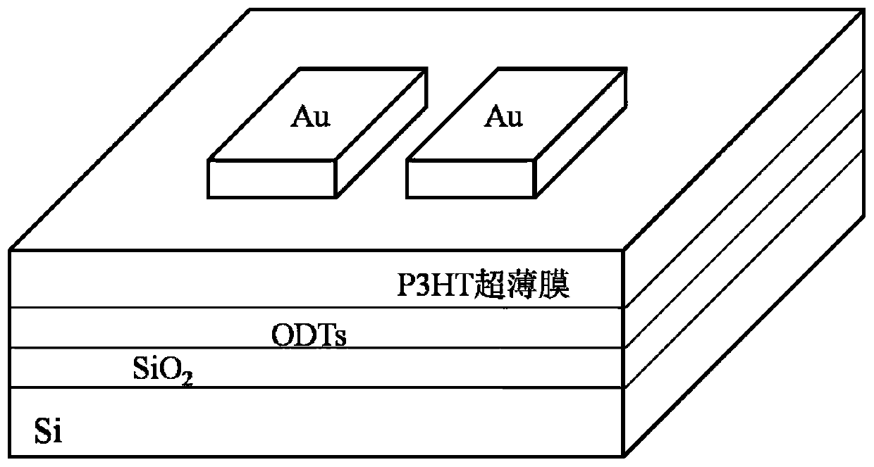
[0032] (2) Wash the n-type silicon wafer with a concentrated sulfuric acid-hydrogen peroxide mixed solution and use it as a substrate; spin-coat the blended solution on the substrate at a speed of 2000 rpm and vacuum dry it at room temperature for 12 hours by spin coating Form a double-layer film with PMMA film as the bottom layer and P3HT film as the top layer;

[0033] (3) Take a silicon wafer with silicon dioxide on the surface (and the surface silicon dioxide layer is modified by octadecylsilane (ODTs)) as a substrate, and float the d...

Embodiment 2

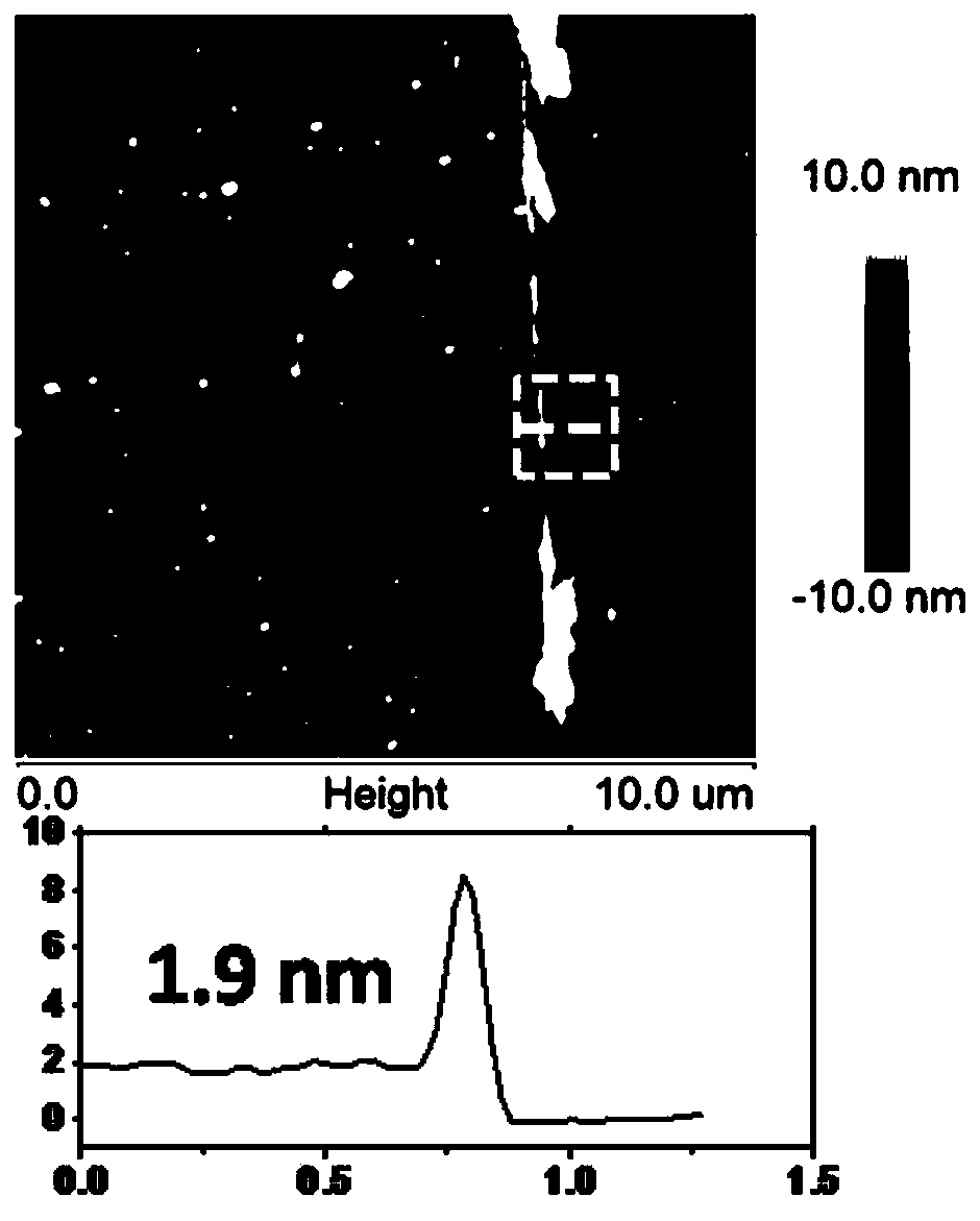
[0040] In this example, P3HT ultra-thin films were prepared in the same manner as in Example 1, except that the mass ratios of P3HT and PMMA in step (1) were sequentially modified to 1:10, 1:20 and 1:40. Figure 6 Shown are the atomic force microscope images of the obtained P3HT ultra-thin films under the corresponding conditions, and it can be seen that the thicknesses of the obtained P3HT ultra-thin films are 7.4nm, 5.2nm and 2.8nm respectively.

[0041] In this example, a P3HT ultra-thin film organic field-effect transistor sensor was prepared by the same method as in Example 1, and its ammonia gas sensing performance was tested. The results show that the sensitivities of the ultra-thin film organic field-effect transistor sensors prepared under the mass ratio conditions of 1:10, 1:20 and 1:40 are 6.88%, 8.72% and 18.62%, respectively, and the response times are 9.23s and 8.67s, respectively. and 9.62s, the recovery time is 122.79s, 101.33s and 95.57s respectively.

Embodiment 3

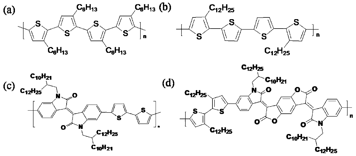
[0043] The present embodiment prepares PIIDBT ultra-thin film and organic field-effect transistor sensor based on it as follows:

[0044] (1) PIIDBT is dissolved in chloroform to form concentration and is the solution A of 1mg / mL, and PMMA is dissolved in chloroform and forms the solution B that concentration is 10mg / mL; Solution A and solution B are mixed uniformly, constitute blending solution, in In the blend solution, the mass ratio of PIIDBT and PMMA was 1:60.

[0045] (2) Wash the n-type silicon wafer with a concentrated sulfuric acid-hydrogen peroxide mixed solution and use it as a substrate; spin-coat the blended solution on the substrate at a speed of 2000 rpm and vacuum dry it at room temperature for 12 hours by spin coating Form a double-layer film with PMMA film as the bottom layer and PIIDBT film as the top layer;

[0046] (3) Take a silicon wafer with silicon dioxide on the surface (and the surface silicon dioxide layer is modified by octadecylsilane (ODTs)) as ...


PUM

PropertyMeasurementUnit
concentrationaaaaaaaaaa
thicknessaaaaaaaaaa
thicknessaaaaaaaaaa

Abstract

The invention discloses an ultrathin film and a preparation method of an organic field-effect transistor sensor based on the ultrathin film. The preparation method is characterized by comprising the following steps: blending a polymer semiconductor material and a polymer insulating material in an organic solvent, and performing spin-coating to form a double-layer film; dissolving to remove the polymer insulating material film by adopting a good solvent, and obtaining the ultrathin film of the polymer semiconductor material; evaporating an electrode on the film, thereby obtaining the organic field-effect transistor sensor. The ultrathin film disclosed by the invention has the advantages of simple operation, high repeatability, low requirements on equipment and process conditions, no need of large precise instruments and equipment and the like; because the active layer has ultrathin thickness, the obtained sensor in the invention has the advantages of high sensitivity, high selectivity, low detection limit and the like, and has an important application prospect in the aspect of improving the sensing property of a gas sensor.

Description

technical field [0001] The invention belongs to the field of organic semiconductor thin films and devices, and in particular relates to an ultra-thin film and a method for preparing an organic field effect transistor sensor based thereon. Background technique [0002] Ultra-thin films generally refer to films whose thickness is less than 10 nm. Ultra-thin-film devices use less material, and when used as the active layer of a gas sensor, they have the advantages of high responsivity, good sensitivity, and fast response recovery. [0003] There are only a few reports on the known preparation methods of ultra-thin films, including the Langmuir-Blodgett (LB) method, self-assembly and impregnation methods, and the materials used are also limited to small molecular materials. In addition, the preparation of ultra-thin films by the solution method has relatively strict requirements on the properties of the materials and the properties of the substrate surface, which is also one of...

Claims


Application Information

Patent Timeline
Patent Type & Authority Patents(China)
IPC IPC(8): G01N27/414
Inventor 王晓鸿邱龙臻葛丰
Owner HEFEI UNIV OF TECH
Why Eureka
Try Eureka