Semiconductor alloy film with continuously and gradually changing component, and preparation method and application of semiconductor alloy film
A technology of alloy film and semiconductor, which is applied in the direction of semiconductor devices, electrical components, circuits, etc., can solve the problems of heavy workload and prone to accidental errors, and achieve the effects of less time-consuming, good stability, and favorable charge transmission
- Summary
- Abstract
- Description
- Claims
- Application Information
AI Technical Summary
Problems solved by technology
Method used
Image

Examples
Embodiment 1
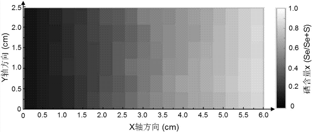
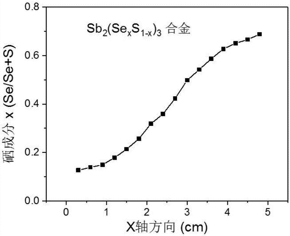
[0044] Sb with continuous gradient of composition 2 (Se x S 1-x ) 3 Semiconductor alloy thin film and its preparation method, wherein the percentage composition of selenium varies from 0.09 to 0.84. Specifically include the following steps:
[0045] (1) Selection and processing of the substrate: cut the FTO into a size of 6×2.5cm 2 For cleaning, use deionized water, acetone, and absolute ethanol for ultrasonic decontamination, then blow dry with high-purity nitrogen, and after UV and ozone treatment for 20 minutes, prepare 60nm TiO by spray pyrolysis on FTO 2 The thin film, as the substrate on which the alloy was deposited, was then heated on a hot stage at 450°C for 10 minutes.
[0046] (2) Preparation of evaporation source: Weigh 0.23g of antimony sulfide and 0.45g of antimony selenide respectively, use a 50-mesh sieve to sieve the two kinds of powders separately, remove the oversized particles, and then sprinkle the two kinds of powders evenly In size 2.5 x 2.5cm 2 a...
Embodiment 2
[0051] Bi with continuous gradient of composition 2 (Se x S 1-x ) 3 Semiconductor alloy thin film and its preparation method, wherein the percentage composition of selenium varies from 0.12 to 0.69. Specifically include the following steps:
[0052] (1) Selection and processing of the substrate: this step is the same as step (1) in Embodiment 1.
[0053] (2) Preparation of evaporation source: Weigh 0.26g of bismuth sulfide and 0.66g of bismuth selenide respectively, use a 50-mesh sieve to sieve the two kinds of powders separately, remove the oversized particles, and then spread the two kinds of powders evenly In size 2 x 2.5cm 2 and 4×2.5cm 2 On the glass plane, the density of its distribution is 0.10mmol / cm 2 .
[0054] (3) Preparation of the semiconductor alloy thin film: this step is the same as step (3) in Example 1.
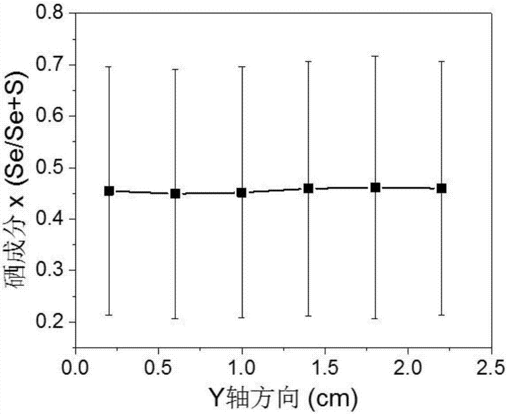
[0055] The change range of the selenium component in the obtained alloy on the X-axis direction is 0.12-0.69. Since different materials have differ...
Embodiment 3
[0057] amorphous Sb 2 (Se x S 1-x ) 3 Semiconductor alloy thin film and its preparation method. Specifically include the following steps:
[0058] (1) Selection and processing of the substrate: this step is the same as step (1) in Embodiment 1.
[0059] (2) Preparation of evaporation source: This step is the same as step (2) in Example 1.
[0060] (3) prepare this semiconductor alloy thin film: according to such as Image 6 The schematic diagram of the structure places the antimony sulfide evaporation source 5, the antimony selenide evaporation source 7 and the substrate sample 8. The two planar evaporation sources are spliced on the aluminum nitride sheet 6 and placed at the bottom of the tray support 3, and the substrate 8 is upside down on the On the tray support 3, ensure that the distance between the substrate and the evaporation source is 1 cm, add a ceramic heat-conducting cover plate 9 on the back of the substrate (here replace the graphite heat-conducting cove...
PUM
| Property | Measurement | Unit |
|---|---|---|
| length | aaaaa | aaaaa |
| width | aaaaa | aaaaa |
| thickness | aaaaa | aaaaa |
Abstract
Description
Claims
Application Information
 - R&D
- Intellectual Property
- Life Sciences
- Materials
- Tech Scout
- Unparalleled Data Quality
- Higher Quality Content
- 60% Fewer Hallucinations
Browse by: Latest US Patents, China's latest patents, Technical Efficacy Thesaurus, Application Domain, Technology Topic, Popular Technical Reports.
© 2025 PatSnap. All rights reserved.Legal|Privacy policy|Modern Slavery Act Transparency Statement|Sitemap|About US| Contact US: help@patsnap.com