Transient voltage suppressor (TVS) chip and manufacturing method

A technology of transient voltage suppression and manufacturing method, applied in semiconductor/solid-state device manufacturing, circuits, electrical components, etc., can solve problems such as the inability to meet the production requirements of high-voltage chips above 400V, and improve anti-surge capability and reliability. , Improve the pressure resistance performance, increase the effect of the structure

Pending Publication Date: 2017-11-14
杭州东沃电子科技有限公司
View PDF12 Cites 4 Cited by
  • Summary
  • Abstract
  • Description
  • Claims
  • Application Information

AI Technical Summary

Problems solved by technology

In the published literature, none of them can meet the production requirements of high-voltage chips above 400V

Method used


Image

  • Transient voltage suppressor (TVS) chip and manufacturing method
  • Transient voltage suppressor (TVS) chip and manufacturing method

Examples


Embodiment 1

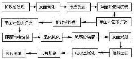
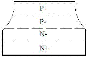
[0023] Embodiment 1: with reference to attached figure 1 and 2 A method for manufacturing a transient voltage suppressor (TVS) chip is further described in detail.

[0024] Pre-diffusion treatment: N-type single crystal silicon wafers are used as raw materials, and the surface of the silicon wafers is chemically treated through acid, alkali, deionized water ultrasonic cleaning and other processes.

[0025] Oxidation: grow a layer of oxide layer on the silicon wafer that has been pre-diffused in an oxidation furnace at 1100-1200 °C.

[0026] Photolithography: Apply gluing, exposure, development, and deoxidation to the oxidized silicon wafer, and engrave a diffusion pattern on the front side in one direction.

[0027] Phosphorus deposition in single-sided open tubes. The single-sided open-tube ammonium dihydrogen phosphate aqueous source deposition process is adopted. The high-purity ammonium dihydrogen phosphate powder is dissolved in deionized water to form an aqueous solut...


PUM


Abstract

The invention discloses a transient voltage suppressor (TVS) chip and a manufacturing method. The transient voltage suppressor (TVS) chip and the manufacturing method have the advantages that: an auxiliary channel structure is designed in a region near a chip table-board, an N-type base depletion layer is limited within a base region when a highest reverse voltage is applied externally, a breakdown voltage of the auxiliary channel structure is higher than a breakdown voltage of a main body junction, so that a main body junction region is broken down at first, a leak current is distributed in the main body junction region, and an auxiliary junction region is not broken down, thereby improving the voltage resistance of a high-voltage transient voltage suppressor, and enhancing surge resistance and reliability of the transient voltage suppressor; a P-type region depletion layer structure is additionally arranged, thus a concentration structure curve of a P-type diffusion region is changed, and a highest reverse voltage resistance value of the device is increased to 800 V or more by utilizing additional voltage resistance of the depletion layer width of the P-type diffusion region; the width of an N+ region is increased; a high-conductivity region is widened, the capability of the N+ region in emitting electrons to the N base region is enhanced, and the positive peak pressure drop of the chip is reduced to 1.22 V and below.

Description

technical field [0001] The invention relates to the technical field of crystal diode chips, in particular to a transient voltage suppressor (TVS) chip and a manufacturing method. Background technique [0002] Transient voltage suppression diode is a safety protection device. This kind of device is used in the circuit system to shunt and clamp the instantaneous surge voltage pulse in the circuit, which can effectively reduce the high-voltage pulse generated by the inductive element due to lightning and switching on and off in the circuit, and avoid high-voltage The pulse damages the equipment and ensures the safety of people and property. At present, the domestic transient voltage suppressor chip manufacturing technology has been reported, such as CN101621002B, titled "a kind of manufacturing method of low-voltage transient voltage suppressor diode chip" is characterized in that: the manufacturing method of the low-voltage transient voltage suppressor diode chip is : a. Sel...

Claims


Application Information

Patent Timeline
Patent Type & Authority Applications(China)
IPC IPC(8): H01L29/861H01L21/329
CPCH01L29/66136H01L29/861
Inventor 朱世良余挺
Owner 杭州东沃电子科技有限公司
Why Eureka
Try Eureka