Compound semiconductor metal contact electrode

A metal contact and semiconductor technology, applied in the direction of semiconductor devices, circuits, electrical components, etc., can solve the problems of fuzzy boundaries of contact resistance electrodes, high manufacturing costs, device failure, etc., to achieve lateral uniformity and stability improvement, production Reduced manufacturing cost and beneficial effect on device size

Inactive Publication Date: 2017-11-28
SUZHOU LIANG DONGXIN MICROELECTRONICS CO LTD
View PDF3 Cites 2 Cited by
  • Summary
  • Abstract
  • Description
  • Claims
  • Application Information

AI Technical Summary

Problems solved by technology

However, in addition to the disadvantages of high manufacturing costs caused by raw materials such as precious metal platinum Pt, gold germanium AuGe and gold Au, these structures also have defects in electrical conductivity and stability; for example, although titanium Ti can improve metal and semiconductor Adhesive strength, but the energy band barrier formed by the contact between Ti and semiconductor is high, so it must be combined with high doping (~10 19 /cm 3 ) semiconductor can form a low-resistance electrical channel, and it still exhibits the characteristics of Schottky connection with the low-doped semiconductor epitaxial layer, which cannot be used as an ideal ohmic connection thick electrode; The process can form a semiconductor-metal transition layer with extremely low contact resistance with the semiconductor in direct contact with it, and the adhesion is very good due to the interpenetration between the semiconductor and metal, but the compound semiconductor metal layer will not only extend vertically during the heat treatment proces

Method used


Image

  • Compound semiconductor metal contact electrode

Examples


Embodiment

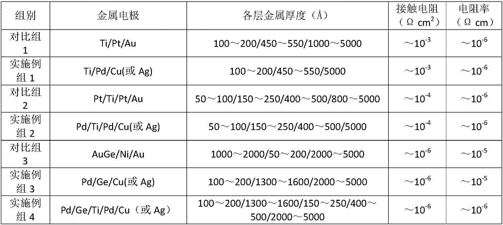
[0022] Prepare metal contact electrodes with the above four structures, that is, prepare Ti / Pd / Cu (or Ag), Pd / Ti / Pd / Cu (or Ag) and alloy metal electrodes Pd / Ge / Cu (or Ag), Pd / Metal contact electrodes with four structures of Ge / Ti / Pd / Cu (or Ag) are used as an embodiment group; metal contact electrodes are prepared with three structures in the prior art, namely preparing Ti / Pt / Au, Pt / Ti / Pt / Au and AuGe / Ni / Au metal contact electrodes with three structures were used as comparison groups.

[0023] By doping concentration ~ 10 19 / cm 3 Thickness is On the n-GaAs test sheet, after photolithography, electron beam evaporation and organic solvent stripping of various metal electrodes to form patterns, adopt the method of "transmission line measurement" to obtain various non-alloy contact electrodes and alloy heat treatment process (He, 250-400°C, 1-3 minutes), the metal contact resistance of the alloy contact electrode was measured, and the intrinsic resistance was measured by comb...


PUM


Abstract

The invention belongs to the technical field of a semiconductor, and discloses a compound semiconductor metal contact electrode. Platinum Pt and gold germanium AuGe in the conventional non-alloy metal electrodes Ti/Pt/Au, Pt/Ti/Pt/Au and alloy type metal electrodes AuGe/Ni/Au are replaced by palladium Pd or palladium germanium Pd/Ge, and top layer noble metal Au is replaced by copper Cu or silver Ag to obtain two kinds of metal contact electrodes which comprise a metal conductive layer and a bonding layer, and comprise a metal conductive layer, a diffusion blocking layer and a bonding layer, wherein the metal conductive layer is a Cu or Ag layer; the diffusion blocking layer is a Pd or Ti/Pd layer; and the bonding layer is a Ti, Pd or Pd/Ge layer. The compound semiconductor metal contact electrode disclosed in the invention has the advantages of low contact resistance, high intrinsic conductivity, high thermal stability, strong adhesive force in connection with the semiconductor, low production and manufacturing cost and the like.

Description

technical field [0001] The invention relates to the technical field of semiconductors, in particular to a compound semiconductor metal contact electrode. Background technique [0002] Smartphones are rapidly entering the era of 4G and 5G, and driven by the Internet of Things industry, multi-mode and multi-frequency microwave RF power devices based on gallium arsenide as III-V compound semiconductors are due to their high electron mobility, high power, and high frequency. , low noise, high gain, anti-natural radiation and many other excellent performances have quickly become mainstream devices in high-end communication electronic products, lighting, military aviation and other fields. The contact resistance between the semiconductor and the metal electrode in this type of high-end electronic device and the conductivity of the metal electrode itself determine and affect whether this type of semiconductor device can achieve the high frequency, high speed, high current density, ...

Claims


Application Information

Patent Timeline
IPC IPC(8): H01L29/49
CPCH01L29/495
Inventor 任华程岸汪耀祖杨斌
Owner SUZHOU LIANG DONGXIN MICROELECTRONICS CO LTD
Why Eureka
Try Eureka