
A three-dimensional micro-nano structure electrochemical induction processing method

A technology of micro-nano structure and processing method, applied in the field of three-dimensional micro-nano structure electrochemical induction processing, can solve the problems of expensive processing equipment, expensive energy beam equipment, low processing efficiency, etc., achieve simple and easy processing technology, and reduce processing complexity Degree, the effect of improving processing efficiency

Active Publication Date: 2019-04-30
HARBIN INST OF TECH +1
View PDF8 Cites 0 Cited by
  • Summary
  • Abstract
  • Description
  • Claims
  • Application Information

AI Technical Summary

Problems solved by technology

Both electron beam lithography and LIGA technology require multi-layer overlay, the processing technology is complicated, and the processing equipment is expensive
Three-beam direct writing technology is energy beam processing, energy beam equipment is relatively expensive, and modulation is difficult, and has the disadvantages of low processing efficiency and high cost
However, the relationship between the tool electrode current, the distance between the tool and the workpiece, and the removal depth is complex, and it is difficult to accurately modulate the removal rate by controlling related parameters. Currently, it is only used for simple two-dimensional structure processing.

Method used


Image

  • A three-dimensional micro-nano structure electrochemical induction processing method
  • A three-dimensional micro-nano structure electrochemical induction processing method
  • A three-dimensional micro-nano structure electrochemical induction processing method

Examples


specific Embodiment approach 1

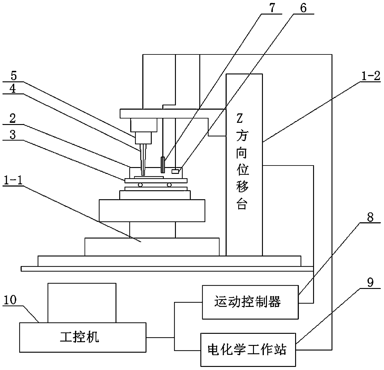
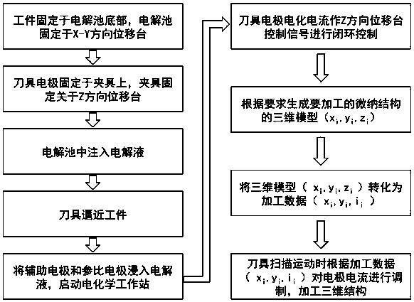
[0031] Specific implementation mode one: as figure 1 and figure 2 As shown, this embodiment describes a three-dimensional micro-nano structure electrochemical induction processing method, and the processing method includes the following steps:

[0032] Step (1): Fix the workpiece 3 to be processed on the bottom of the electrolytic cell 2 in the electrochemical system, and then fix the electrolytic cell 2 on the horizontal displacement table 1-1 in the X-Y direction;

[0033] Step (2): Fixing the micro-nano size cutter electrode 4 (referred to as the cutter electrode) on the fixture 5, and then fixing the fixture 5 on the Z-direction displacement table 1-2;

[0034] Step (3): Inject electrolyte solution into the electrolytic cell 2, so that the electrolyte solution does not pass through the workpiece 3 to be processed;

[0035] Step (4): controlling the micro-nano-sized tool electrode 4 to approach the workpiece 3;

[0036] Step (5): Immerse the auxiliary electrode 6 and th...

specific Embodiment approach 2

[0041] Specific implementation mode two: as figure 2 As shown, this embodiment is a further description of specific embodiment 1. In step (1), the material of the workpiece 3 to be processed is metal or semiconductor; the metal is magnesium, aluminum, iron, titanium, Vanadium or copper, or an alloy of at least two of the above materials; the semiconductor is silicon, germanium, gallium arsenide, gallium phosphide, indium phosphide, zinc sulfide or cadmium telluride, or at least two of the above materials combination.

specific Embodiment approach 3

[0042] Specific implementation mode three: as figure 2As shown, this embodiment is a further description of Embodiment 1. In step (2), the micronano-sized cutter electrode 4 is a platinum metal or platinum-iridium alloy disk electrode with a diameter of 0.01-100 um. In this embodiment, different precision machining can be performed according to the size of the specific micro-nano-sized cutter electrode 4 .


PUM


Abstract

The invention discloses an electrochemical induction processing method for three dimensional micro-nano structure, and belongs to the field of micro-nano structure processing. The processing method comprises the following steps that a to-be-processed workpiece is fixed at the bottom of an electrolytic tank of an electrochemical system, and then the electrolytic tank is fixed on an X-Y direction horizontal displacement table; an micro-nano sized tool electrode is fixed on a fixture, and then the fixture is fixed on an Z-direction displacement table, and electrolyte is injected into the electrolytic tank until the to-be-processed workpiece is soaked in the electrolyte completely; the micro-nano sized tool electrode is controlled to approach the to-be-processed workpiece, the Z-direction micro-moving displacement table is set as a close-loop mode, and micro-nano sized tool electrode electrification current serves as a close-loop signal; and when the micro-nano sized tool electrode is in scanning movement, electrochemical current of the micro-nano sized tool electrode can be modulated in real time according to the three-dimensional profile of a preprocessing structure, and finally a predetermined three dimensional micro-nano structure can be processed on the surface of the to-be-processed workpiece. According to the electrochemical induction processing method for the three dimensional micro-nano structure, molding at a time is achieved, thus the processing complexity is reduced greatly, and the processing efficiency is improved.

Description

technical field [0001] The invention relates to the field of micro-nano structure processing, in particular to a three-dimensional micro-nano structure electrochemical induction processing method. Background technique [0002] Micro-nano structure processing is the core technology in the fields of micro-nano optical components, micro-electromechanical systems, micro-total analysis systems and precision optics. At present, the three-dimensional micro-nano structure processing methods mainly include: electron beam lithography, LIGA (lithography, electroplating and casting process), three-beam direct writing technology (electron beam, focused ion beam, laser beam), micro-milling, micro-EDM Wait. Electron beam lithography and LIGA technology both require multi-layer overlay, the processing technology is complicated, and the processing equipment is expensive. The three-beam direct writing technology is energy beam processing, and the energy beam equipment is relatively expensiv...

Claims


Application Information

Patent Timeline
Patent Type & Authority Patents(China)
IPC IPC(8): B23H5/06
CPCB23H5/06
Inventor 闫永达詹东平韩联欢曹永智胡振江赵学森
Owner HARBIN INST OF TECH
Learn More