Perovskite wideband flexible light detector and a preparation method thereof

A photodetector and perovskite technology, applied in semiconductor/solid-state device manufacturing, photovoltaic power generation, electric solid-state devices, etc., can solve the problems of inflexible preparation, heavy quality, and light absorption defects, and achieve enhanced photoresponse performance and The effect of detection rate

Inactive Publication Date: 2017-12-01
SHAANXI NORMAL UNIV
View PDF4 Cites 7 Cited by
  • Summary
  • Abstract
  • Description
  • Claims
  • Application Information

AI Technical Summary

Problems solved by technology

But these photodetectors have serious drawbacks: opaque, inflexible and heavy
However, the light absorption defects of organic h

Method used


Image

  • Perovskite wideband flexible light detector and a preparation method thereof
  • Perovskite wideband flexible light detector and a preparation method thereof
  • Perovskite wideband flexible light detector and a preparation method thereof

Examples


preparation example Construction

[0030] A kind of preparation method of the broadband flexible photodetector of perovskite of the present invention, comprises the following steps:

[0031] Step 1, preparing a perovskite film on a flexible PET substrate by vacuum deposition or solution spin coating, printing and spraying;

[0032] The specific method is: select a regular flexible substrate of high-quality ethylene terephthalate (PET), ultrasonically clean it in acetone, ethanol, and isopropanol for 15 minutes, and then dry it with nitrogen and put it into oxygen plasma treatment. 5 minutes standby;

[0033] The perovskite film was prepared on the cleaned PET substrate by vacuum deposition or solution spin coating, printing and spraying. Perovskite films range in thickness from 100 nanometers to 5 micrometers thick.

[0034] Step 2, preparing an up-conversion particle layer on the perovskite film by spin coating or printing, and the thickness of the up-conversion particle layer is 10-50 nanometers;

[0035] ...

Embodiment 1

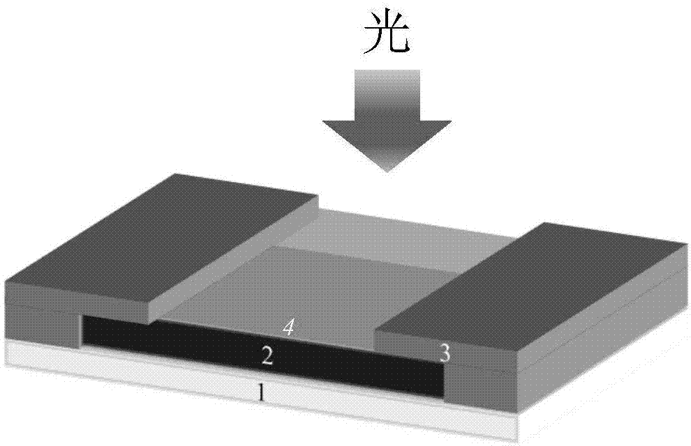
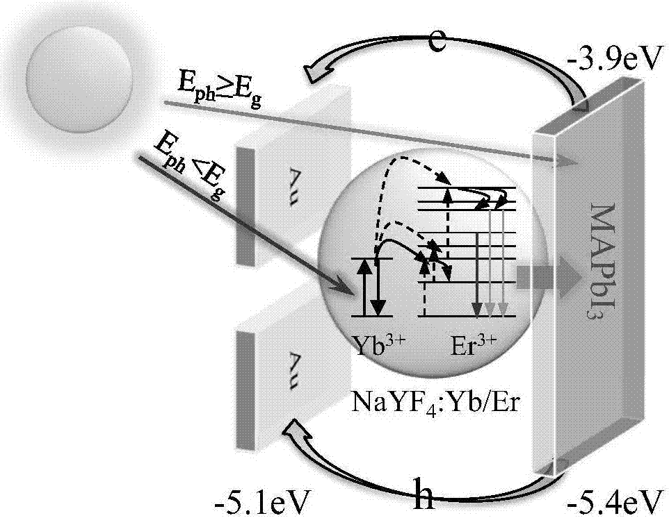
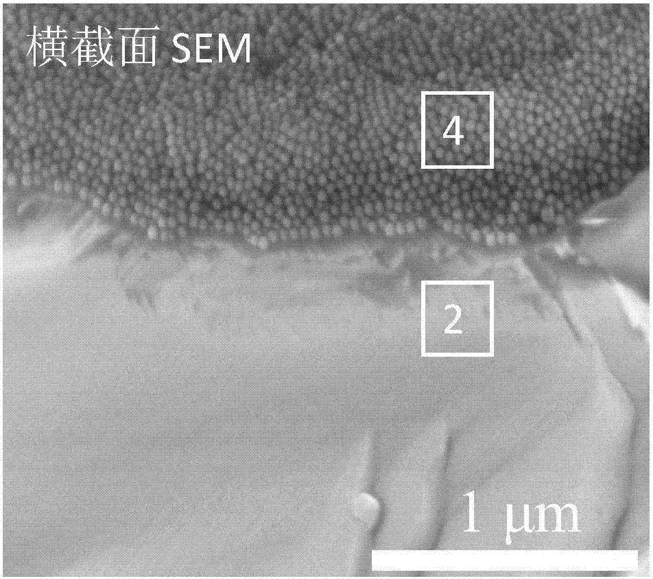
[0041] The best embodiment of the present invention adopts PET transparent film as substrate, and MAPbI 3 A perovskite nitrogen-nitrogen dimethylformamide (DMF, concentration of 1M) solution was scraped on a PET substrate to form an oriented single crystal fiber perovskite film with a thickness of 3 microns. NaYF 4 : The upconversion particle layer of Yb-Er is uniformly dispersed in cyclohexane solvent by means of ultrasonic vibration. A layer of NaYF with a thickness of 20 nm was prepared by spin coating on the perovskite film 4 :Yb-Er upconversion particle layer. Place the perovskite / upconversion particle composite at Figure 4 shown.

Embodiment 2

[0043] Using PET transparent film as the substrate, the MAPbI 3 The perovskite solution was deposited on a PET substrate to form a perovskite film with a thickness of 100 nanometers. NaYbF 4 : The upconversion particle layer of Yb-Er is uniformly dispersed in cyclohexane solvent by means of ultrasonic vibration. Fabrication of a layer of NaYbF on perovskite film by spin coating 4 : Yb-Er up-conversion particle layer with a thickness of 10 nm. Place the perovskite / upconversion particle composite at <70% humidity and heat anneal at 100°C for 10 minutes. A back electrode (Au, 80 nm) was vacuum-evaporated on the surface of the up-conversion particle. Other steps are identical with embodiment 1.


PUM

PropertyMeasurementUnit
Thicknessaaaaaaaaaa
Thicknessaaaaaaaaaa
Thicknessaaaaaaaaaa

Abstract

The invention discloses a perovskite wideband flexible light detector and a preparation method thereof. The flexible light detector consists of a flexible substrate and the following elements arranged sequentially on the flexible substrate: a perovskite film, an upconversion particle layer with a thickness of 10-50 nanometers, and a metal electrode disposed directly on the upconversion particle layer. The preparation method comprises the following steps: Step 1: preparing a perovskite crystal by any one of following methods on the flexible substrate: vacuum depositing, solution spin coating, printing and spraying to form a perovskite film; Step 2: performing spin coating or printing directly on the perovskite film to prepare upconversion particles with a thickness of 10-50 nanometers to obtain an upconversion particle layer and obtaining a perovskite/upconversion particle composite composed of the perovskite film and the upconversion particle layer; and Step 3, performing the vacuum evaporation directly on the perovskite/upconversion particle composite for a metal electrode, and preparing out a perovskite wideband flexible light detector able to respond the visible-near infrared band.

Description

technical field [0001] The invention relates to a perovskite photodetector, in particular to a perovskite wide-band flexible photodetector and a preparation method thereof. Background technique [0002] Photodetectors are widely used in image sensing, optical fiber transmission, spectroscopy and biomedicine. At present, photodetectors in the ultraviolet, visible and infrared regions are made of SiC, Si and HgCdTe, respectively. But these photodetectors have serious drawbacks: opaque, inflexible and heavy. Therefore, a new generation of rollable and portable high-efficiency photodetectors has become an important research direction. Organohalogen perovskites have the advantages of wide absorption band, long migration distance of photogenerated carriers and low density of defect states, and have become important materials for the preparation of a new generation of high-efficiency optoelectronic devices. The basic structure of photodetectors based on organic halogen perovskit...

Claims


Application Information

Patent Timeline
IPC IPC(8): H01L51/42H01L51/46H01L51/48
CPCH10K30/35H10K2102/00Y02E10/549
Inventor 赵奎李剑波沈颖丽刘渝城石峰刘生忠
Owner SHAANXI NORMAL UNIV
Why Eureka
Try Eureka