A micron line array photodetector and its preparation method
A photodetector, micro-wire technology, applied in semiconductor devices, final product manufacturing, sustainable manufacturing/processing, etc., can solve the problems of undetectable detectors, unfavorable practical applications, and easy to be affected by external disturbances.
- Summary
- Abstract
- Description
- Claims
- Application Information
AI Technical Summary
Problems solved by technology
Method used
Image
Examples
preparation example Construction
[0060] The present invention also provides a method for preparing a micron line array photodetector described in the above technical solution, comprising the following steps:
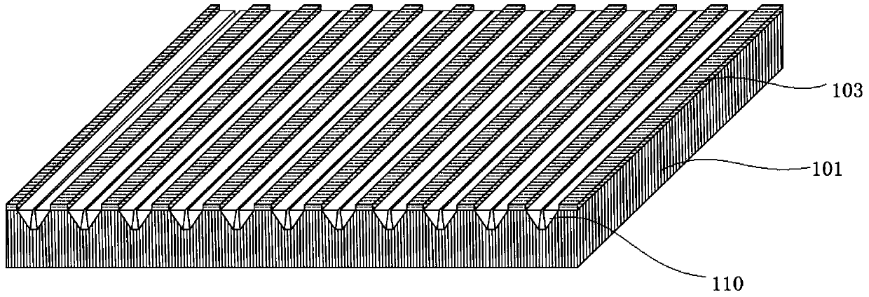
[0061] (1) Etching a silicon wafer with an insulating layer to obtain a patterned substrate with a plurality of parallel groove arrays;
[0062] (2) In the step (1), gallium nitride micro-wires are epitaxially grown on the inner side walls of the trenches, and a gallium nitride micro-wires are respectively grown on the two inner side walls of each trench to form an epitaxial structure on the substrate surface ;
[0063] (3) In the step (2), both ends of the gallium nitride microwires are covered with Schottky contact type metal electrodes to obtain a micrometer wire array photodetector.
[0064] The invention etches the silicon wafer with the insulating layer to obtain a patterned substrate with a plurality of parallel trench arrays. In the present invention, there is no special limitation on the sour...
Embodiment 1
[0076] The structure of the micron line array ultraviolet photodetector prepared in this embodiment is as follows: Figure 1~5 As shown, the optical micrograph of the micron line array photodetector in the present embodiment is as follows Figure 11 Shown: the substrate material 100 is a silicon wafer with a crystal orientation of , the silicon wafer is an intrinsic material, and the resistivity is as high as 10 4 Ω·cm; the insulating layer 103 covers the silicon surface and is a layer of SiO with a thickness of 300nm 2 , the width of the insulating layer is 5 microns; the width of the trench is 2 microns; the epitaxial structure 110 is epitaxial on the sidewall of the trench 102 of the high-resistance silicon substrate, and the epitaxial structure successively includes an aluminum nitride buffer layer 111 with a thickness of 30 nm and a gallium nitride epitaxial layer 112 with a thickness of 300nm, the AlN buffer layer 111 is stacked on the trench side 102 of the intrinsic s...
Embodiment 2
[0097] According to the method of embodiment 1, micron line array photodetectors are prepared, and the specific structure is as follows Figure 6-10 Shown: the substrate material 100 is a 2-inch intrinsic silicon wafer material with a crystal orientation of , and the resistivity is as high as 10 3 Ω·cm; the insulating layer 103 covers the silicon surface and is a layer of SiO with a thickness of 150nm 2 The epitaxial structure 110 is epitaxial on the sidewall of the high-resistance silicon substrate trench 102, and its epitaxial structure includes an aluminum nitride buffer layer 111 and a gallium nitride epitaxial layer 112 in sequence, and the AlN buffer layer 111 is stacked on the intrinsic On the groove side 102 of the silicon substrate, the gallium nitride epitaxial layer 112 is stacked on the aluminum nitride buffer layer 111; since the crystal orientation of the substrate is different from that of Embodiment 1, the cross-sectional shape of the groove will change from ...
PUM
 Abstract
Description
Claims
Application Information


