
Organic field effect transistor-based ammonia gas sensor and preparation method therefor

An ammonia sensor and organic field technology, applied in the field of sensors, can solve the problems of high manpower and material consumption and high cost, and achieve the effects of saving manpower and material resources, no need to extract, and improving response rate

Active Publication Date: 2018-01-09
UNIV OF ELECTRONICS SCI & TECH OF CHINA
View PDF7 Cites 20 Cited by
  • Summary
  • Abstract
  • Description
  • Claims
  • Application Information

AI Technical Summary

Problems solved by technology

[0004] In order to solve the problem of high cost of the existing field effect transistor gas sensor due to the use of materials that consume a lot of manpower and materials, the present invention provides an ammonia gas sensor based on organic field effect transistor and its preparation method, which has the advantages of simple preparation process, It has the characteristics of low production cost, green and environmental protection, and has the characteristics of high sensitivity, high stability and long life in the atmospheric environment

Method used


Image

  • Organic field effect transistor-based ammonia gas sensor and preparation method therefor
  • Organic field effect transistor-based ammonia gas sensor and preparation method therefor

Examples


preparation example Construction

[0035] A method for preparing an organic field effect transistor ammonia sensor, comprising the following steps:

[0036] ① Clean the substrate layer with detergent, acetone solution, deionized water and isopropanol solution, and dry it with nitrogen after cleaning;

[0037] ②Preparing a gate electrode on the surface of the substrate layer;

[0038] ③ Prepare a dielectric layer on the gate electrode;

[0039] ④ Ultrasonic mixing of egg white protein and soluble organic semiconductor material in proportion; using the mixed solution to prepare an organic semiconductor layer on the dielectric layer;

[0040] ⑤ Prepare source and drain electrodes on the organic semiconductor layer.

[0041] In the above step ③, the dielectric layer is prepared by one of the methods of spin coating, roll coating, drop film, embossing, printing or spray coating.

[0042] In the above step ④, the organic semiconductor layer is prepared by one of the methods of dynamic spin coating, roller coating,...

Embodiment 1

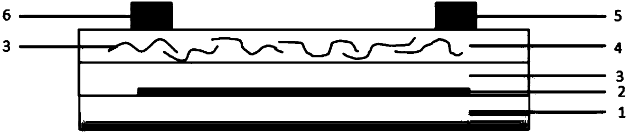
[0045] Such as figure 1 The bottom gate top contact structure is shown, the gate electrode 2, the source electrode 5 and the drain electrode 6 are all silver nanowires, the dielectric layer 3 is made of egg white protein, and the thickness is 200nm; the organic semiconductor layer 4 is poly 3-hexylthiophene (P3HT) is mixed with egg white protein (10% by mass), and the thickness is 30nm. A field effect transistor gas sensor with high sensitivity and high stability can be realized by using the structure.

[0046] ① Clean the substrate layer with detergent, acetone solution, deionized water and isopropanol solution, and dry it with nitrogen after cleaning;

[0047] ② Preparation of gate electrodes on the surface of the substrate layer;

[0048] ③Preparing a dielectric layer on the gate electrode;

[0049]④ Ultrasonic mixing of egg white protein and soluble organic semiconductor material in proportion. Use the mixed solution on the dielectric layer

[0050] Prepare an organic...

Embodiment 2

[0053] Such as figure 1 The bottom gate top contact structure is shown, the gate electrode, source electrode and drain electrode are all copper nanowires, the dielectric layer is made of duck egg white protein, and the thickness is 500nm; the organic semiconductor layer is Tips-pentacene (Tips-pentacene) It is formed by mixing with egg white protein (accounting for 15% by mass), and the thickness is 30nm. A field effect transistor gas sensor with high sensitivity and long life can be realized by using the structure.

[0054] ① Clean the substrate layer with detergent, acetone solution, deionized water and isopropanol solution, and dry it with nitrogen after cleaning;

[0055] ②Preparing a gate electrode on the surface of the substrate layer;

[0056] ③Preparing a dielectric layer on the gate electrode;

[0057] ④ Ultrasonic mixing of egg white protein and soluble organic semiconductor material in proportion. Using the mixed solution to prepare an organic semiconductor laye...


PUM

PropertyMeasurementUnit
Thicknessaaaaaaaaaa
Thicknessaaaaaaaaaa
Thicknessaaaaaaaaaa

Abstract

The invention belongs to the technical field of a sensor, and discloses an organic field effect transistor-based ammonia gas sensor and a preparation method therefor, and aims to solve the problem ofhigh cost of the existing organic field effect transistor-based ammonia gas sensor due to a large amount of consumed manpower and materials. The organic field effect transistor-based ammonia gas sensor comprises a substrate layer, a gate electrode, a dielectric layer and an organic semiconductor layer which are arranged from the bottom up in sequence; the upper end of the organic semiconductor layer is connected with a source electrode and a drain electrode; the ammonia gas sensor is characterized in that the dielectric layer adopts the material of egg white protein; and the organic semiconductor layer is prepared from a soluble organic semiconductor material with 5-15mass% of egg white protein.

Description

technical field [0001] The invention belongs to the technical field of sensors, and in particular relates to an organic field effect tube ammonia sensor based on a biodielectric layer and a biomaterial-doped organic layer and a preparation method thereof. Background technique [0002] Today, with the rapid development of industry, while enjoying the rapid changes brought by the development of science and technology, people have to start paying attention to the negative impact brought by the development of science and technology-environmental pollution. Among them, air pollution is closely related to people's lives. attention. In life, people directly or indirectly release a lot of harmful gases into the atmosphere, such as methane, nitrogen monoxide, nitrogen dioxide, ammonia, sulfur dioxide and hydrogen sulfide, etc., and sometimes even endanger life. Gas sensors based on FETs have become a research hotspot in the field of sensors, and their application to the detection of...

Claims


Application Information

Patent Timeline
IPC IPC(8): H01L51/05H01L51/40G01N27/414
Inventor 于军胜庄昕明范惠东侯思辉
Owner UNIV OF ELECTRONICS SCI & TECH OF CHINA
Learn More