Organic/perovskite bulk heterojunction nanowire photodetector and preparation method thereof

A bulk heterojunction and photodetector technology, applied in semiconductor devices, circuits, electrical components, etc., can solve the problems of perovskite material failure and low device performance, achieve excellent photoelectric performance, low excitation binding energy, The effect of excellent flexibility

Inactive Publication Date: 2018-03-06
CENT SOUTH UNIV
View PDF4 Cites 5 Cited by
  • Summary
  • Abstract
  • Description
  • Claims
  • Application Information

AI Technical Summary

Problems solved by technology

Usually, the perovskite nanowires prepared by our simple solution method are disordered, which will lead to low device performance
Moreover, the perovskite material is very sensitive to water molecules in the air. When exposed to the air, the perovskite material will react with the water in the air, causing the perovskite material to decompose and fail.

Method used


Image

  • Organic/perovskite bulk heterojunction nanowire photodetector and preparation method thereof
  • Organic/perovskite bulk heterojunction nanowire photodetector and preparation method thereof
  • Organic/perovskite bulk heterojunction nanowire photodetector and preparation method thereof

Examples


Embodiment 1

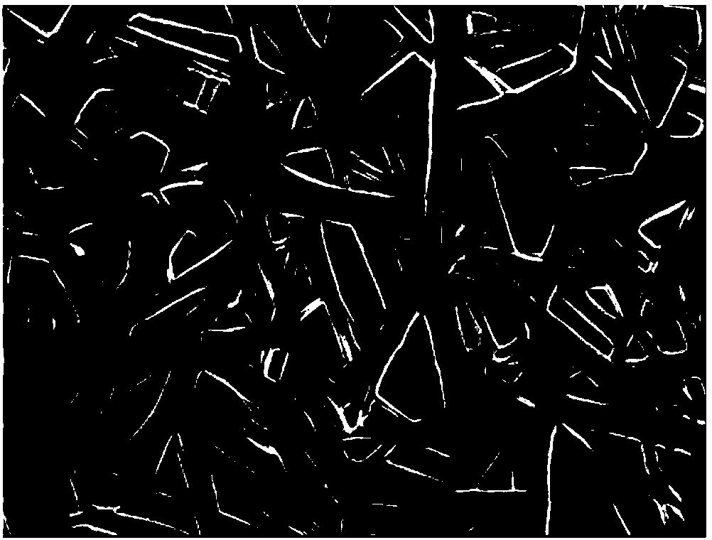
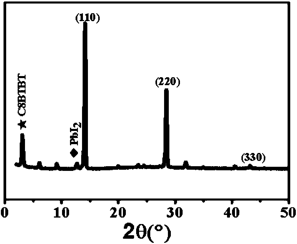
[0039] a kind of like figure 1 The shown perovskite / 2,7-dioctyl[1]benzothieno[3,2-b]benzothiophene bulk heterojunction nanowire photodetector including polyethylene terephthalate Ester (PET) base, CH 3 NH 3 PB 3 / 2,7-dioctyl[1]benzothieno[3,2-b]benzothiophene phase heterojunction nanowire light absorption layer and gold electrode three parts.

[0040] The preparation method on the glass substrate in the present embodiment comprises the following steps:

[0041] (1) Use deionized water, acetone, and absolute ethanol to ultrasonically clean the PET substrate for 20 minutes, then dry it with high-purity gas, and then treat it with UV-ozone for 20 minutes.

[0042] (2) CH 3 NH 3 I:PbI 2 After weighing at a molar ratio of 1:1, CH 3 NH 3 I was dissolved in N-N dimethylformamide, then CH 3 NH 3 I solution with PbI 2 Mix, and finally heat and stir, wherein the heating temperature is 80 degrees, and the stirring time is 10 hours to obtain 550 mg / ml of CH 3 NH 3 PB 3 prec...

Embodiment 2

[0050] a kind of like figure 1 The shown perovskite / 2,7-dioctyl[1]benzothieno[3,2-b]benzothiophene bulk heterojunction nanowire photodetector including polyethylene naphthalate Ester (PEN) base, CH 3 NH 3 PbBr 3 / 2,7-dioctyl[1]benzothieno[3,2-b]benzothiophene phase heterojunction nanowire light absorption layer and silver electrode three parts.

[0051] The preparation method on polyethylene naphthalate (PEN) substrate in the present embodiment comprises the following steps:

[0052] (1) Use deionized water, acetone, and absolute ethanol to ultrasonically clean the PET substrate for 20 minutes, then dry it with high-purity gas, and then treat it with UV-ozone for 20 minutes.

[0053] (2) CH 3 NH 3 Br:PbBr 2 After weighing at a molar ratio of 1:1, CH 3 NH 3 Br was dissolved in N-N dimethylformamide, then the CH 3 NH 3 Br solution and PbBr 2 Mix, and finally heat and stir, wherein the heating temperature is 60 degrees, and the stirring time is 8 hours to obtain 300 ...

Embodiment 3

[0060] a kind of like figure 1 The shown perovskite / 2,7-dioctyl[1]benzothieno[3,2-b]benzothiophene bulk heterojunction nanowire photodetector including polyimide (PI) Base, CH 3 NH 3 PbCl 3-x I x / 2,7-dioctyl[1]benzothieno[3,2-b]benzothiophene phase heterojunction nanowire and aluminum electrode three parts.

[0061] The preparation method on the polyimide (PI) substrate in the present embodiment comprises the following steps:

[0062] (1) Use deionized water, acetone, and absolute ethanol to ultrasonically clean the glass substrate for 20 minutes, then dry it with high-purity gas, and finally treat it with UV-ozone for 20 minutes.

[0063] (2) CH 3 NH 3 I:PbCl 2 After weighing at a molar ratio of 1:1, CH 3 NH 3 I was dissolved in N-N dimethylformamide, then CH 3 NH 3 I solution with PbCl 2 Mix, and finally heat and stir, where the heating temperature is 70°C, and the stirring time is 8h, to obtain 600mg / ml of CH 3 NH 3 PbCl 3-x I x solution.

[0064] (3) Di...


PUM

PropertyMeasurementUnit
sizeaaaaaaaaaa

Abstract

The invention discloses an organic/perovskite bulk heterojunction nanowire photodetector, which comprises three parts, namely a substrate, a perovskite/2,7-dioctyl[1] benzothieno[3,2-b] benzothiophenebulk heterojunction nanowire light absorption layer and an electrode. A preparation method comprises the following steps of preparing the substrate, and cleaning and processing the substrate; preparing a perovskite material solution; preparing perovskite/2,7-dioctyl[1] benzothieno[3,2-b] benzothiophene mixed material precursor solution; preparing a perovskite/2,7-dioctyl[1] benzothieno[3,2-b] benzothiophene bulk heterojunction nanowire by using spin-coating, blade-coating and printing methods to obtain a high-quality light absorption layer; and preparing an electrode by adopting an evaporation or printing method. The product disclosed by the invention has the advantages of being short in response time, high in photoresponsivity and stable in air, and has an important application prospect.

Description

technical field [0001] The invention belongs to the field of optoelectronic devices, and in particular relates to an organic / perovskite bulk phase heterojunction nanowire photodetector and a preparation method thereof. Background technique [0002] Photodetectors refer to optoelectronic devices that can convert incident light signals (infrared, visible, and near-infrared regions) into electrical signals (current or voltage), and are widely used in imaging, communication, spectroscopy, and biomedicine. At present, traditional photodetectors are mainly made of the following typical materials, such as conventional semiconductor materials (silicon, germanium), two-dimensional materials (graphene, molybdenum sulfide), and conjugated polymers. [0003] In recent years, organic-inorganic hybrid halide perovskite materials have gradually developed, which mainly refers to CH 3 NH 3 wxya 3 (X = Cl, Br, I) material. Since this type of perovskite material has excellent semiconducto...

Claims


Application Information

Patent Timeline
Patent Type & Authority Applications(China)
IPC IPC(8): H01L31/09H01L31/0216H01L31/0256H01L31/18
CPCH01L31/0216H01L31/0256H01L31/09H01L31/18H01L2031/0344Y02P70/50
Inventor 阳军亮夏华艳张楚俊童思超王春花
Owner CENT SOUTH UNIV
Why Eureka
Try Eureka