Preparation method of CIGS compound, printing ink and film absorbing layer

A copper indium gallium selenide and compound technology, which is applied in the field of preparing thin film absorbing layers, can solve the problems of selenium component loss, component mismatch, difficult control, etc.

Inactive Publication Date: 2018-05-15
BEIJING APOLLO DING RONG SOLAR TECH
View PDF5 Cites 2 Cited by
  • Summary
  • Abstract
  • Description
  • Claims
  • Application Information

AI Technical Summary

Problems solved by technology

[0003] At present, there are two main methods for the preparation of non-vacuum printing CIGS coating slurry or colloid. First, the chemical synthesis method is used to prepare CIGS nanomaterials and further modulate them into slurry. However, the purity of chemically synthesized CIGS is low, and the prepared CIGS film has a low carrier life. Low, so the battery efficiency of this kind of absorption layer is relatively low at present; second, use four kinds of elemental powders or several kinds of two ternary compound powders to formulate coating raw materials, this kind of slurry will form a quaternary compound when the film is formed and further reacts The reaction is difficult to control. Insufficient reaction will cause component mismatch. At the same time, high reaction temperature will easily cause a large loss of selenium components, so the quality of the prepared CIGS film is poor.
[0004] In addition, the preparation of CIGS thin films with gradual band gaps is beneficial to improve the conversion efficiency of the light-absorbing layer of thin films. However, the current printing and preparation of CIGS thin films is limited to the preparation method of CIGS materials, and most of them are single fixed component CIGS, which is not conducive to the preparation of high-efficiency batteries.

Method used


Image

  • Preparation method of CIGS compound, printing ink and film absorbing layer
  • Preparation method of CIGS compound, printing ink and film absorbing layer
  • Preparation method of CIGS compound, printing ink and film absorbing layer

Examples


Embodiment 1

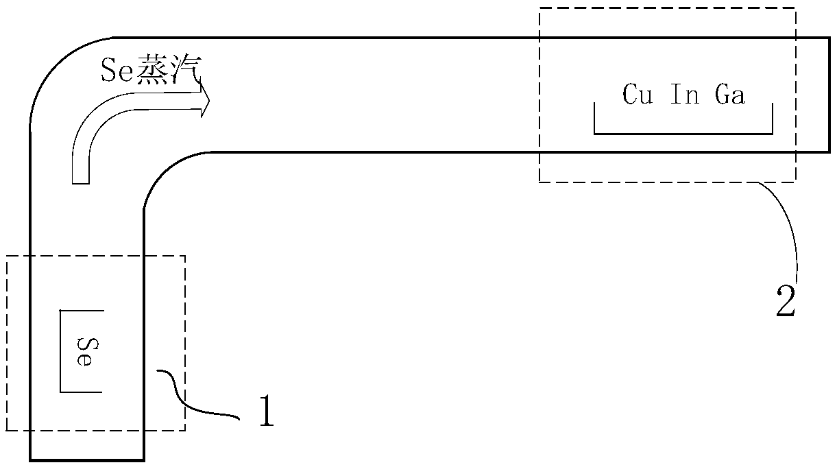
[0049] Such as figure 1 As shown, this embodiment provides a method for preparing copper indium gallium selenide compound, the steps are as follows:

[0050] S1 provides a vacuum container, and the vacuum container includes a high-temperature synthesis zone 1 and a low-temperature evaporation zone 2 arranged at intervals;

[0051] S2 places copper, indium, and gallium in the high-temperature synthesis zone 1, and places selenium in the low-temperature evaporation zone 2;

[0052] S3 heats the copper, indium, and gallium in the high-temperature synthesis zone 1 to a molten state, and heats the selenium in the low-temperature evaporation zone 2 to a gaseous state; the time when the selenium in the low-temperature evaporation zone 2 starts to change to a gaseous state is not earlier than the time when copper indium gallium is melted ;

[0053] S4 heats the high-temperature synthesis zone 1 and the low-temperature evaporation zone 2;

[0054]S5 lowering the temperature of the h...

Embodiment 2

[0065] The present embodiment provides a kind of method for preparing CIGS printing ink, comprises the following steps:

[0066] S1 Grinding the copper indium gallium selenide compound prepared in the above embodiment 1 into powder;

[0067] S2 adding solvent, binder and dispersant to the powder and stirring to form uniformly;

[0068] In S3, the mixture is evaporated by heating or standing to volatilize, and the solvent is removed to form a slurry.

[0069] In S1, the CIGS compound prepared in Example 1 can be ground into nanopowder by using a zirconia planetary ball mill. Of course, the method of pulverizing the CIGS compound is not limited to the zirconia planetary ball mill, and other methods can also be used, as long as the CIGS can be pulverized into Nano powder can be.

[0070] In S2, the copper indium gallium selenide compound powder is mixed with a solvent, a binder and a dispersant; the above mixture is stirred and ultrasonicated to form a uniform mixture. The sol...

Embodiment 3

[0074] This embodiment provides a preparation method for preparing a copper indium gallium selenide light-absorbing layer. The copper indium gallium selenide ink prepared in embodiment 3 is used for coating the slurry on Mo-plated soda lime glass or stainless steel substrate by screen printing. Cloth, the coating method can be intermittent coating or continuous coating according to the overall process requirements of the thin film battery. Transfer the slurry-coated substrate into a continuous sintering furnace for slurry drying and annealing. The drying temperature is 150°C-250°C, the drying time is 3min-5min, the annealing temperature is 450°C-550°C, and the annealing time is 10min-15min , and finally get the absorbing layer with CIGS thin film.

[0075] In this embodiment, the ink prepared in embodiment 3 is on Mo-plated soda-lime glass or stainless steel substrate, and then the slurry is dried, and the liquid binding phase can be evaporated or decomposed during the drying ...


PUM


Abstract

The invention discloses a preparation method of a CIGS compound, printing ink and film absorbing layer. The preparation method of the CIGS compound comprises the following steps that a vacuum container is provided, wherein the vacuum container includes a high temperature synthesis area and a low temperature evaporation area which are arranged in a spaced way; single substances of copper, indium and gallium are arranged in the high temperature synthesis area and the single substance of selenium is arranged in the low temperature evaporation area; the copper, the indium and the gallium of the high temperature synthesis area are heated to the molten state, and the selenium of the low temperature evaporation area is heated to the gaseous state; the time when the selenium of the low temperatureevaporation area starts to turn to the gaseous state is not early than the molten time of the copper, the indium and the gallium; the temperature of the high temperature synthesis area and the low temperature evaporation area is preserved; the temperature of the high temperature synthesis area is reduced to be not lower than the molten temperature of the alloy of the copper, the indium and the gallium and the temperature is preserved, then the temperature of high temperature synthesis area and the low temperature evaporation area is reduced to be lower than 100 DEG C; and the forward temperature gradient between the low temperature evaporation area and the high temperature synthesis area is constantly kept in the steps.

Description

technical field [0001] The invention relates to a method for preparing a copper indium gallium selenide quaternary compound, a method for preparing ink by using the copper indium gallium selenide compound, and a method for preparing a film absorption layer by using the copper indium gallium selenide ink. Background technique [0002] As we all know, CIGS thin-film battery is the most potential thin-film solar cell. At present, the mainstream methods for preparing CIGS in the industry are co-evaporation and magnetron sputtering. Based on the high vacuum of the first two methods, no matter from the equipment or process Therefore, non-vacuum and low-cost CIGS preparation technologies such as printing have been continuously promoted by the industry. [0003] At present, there are two main methods for the preparation of non-vacuum printing CIGS coating slurry or colloid. First, the chemical synthesis method is used to prepare CIGS nanomaterials and further modulate them into slur...

Claims


Application Information

Patent Timeline
Patent Type & Authority Applications(China)
IPC IPC(8): H01L31/18H01L21/673H01L31/0445B22F1/054B22F1/10
CPCH01L31/0445H01L21/673H01L31/18B22F1/054B22F1/10B22F2998/10B22F9/06B22F9/12B22F9/04B22F2007/042B22F3/10B22F3/1021C22C1/0425C22C1/0483C22C9/00H01L31/0749B22F2999/00H01L2924/10821H01L31/0322C22C1/02C22C1/047C01B19/002B01J19/0073B01J12/005C09D11/00B01J2219/00331B01J2219/00594Y02E10/50Y02P70/50H01L31/1864
Inventor 陈腾
Owner BEIJING APOLLO DING RONG SOLAR TECH
Why Eureka
Try Eureka