A kind of preparation method of body centered cubic tantalum coating
A body-centered cubic, tantalum coating technology, applied in the field of material science, can solve problems such as difficulty in promotion, chromic waste water and waste gas cause cancer, increase production costs, etc., to avoid environmental pollution and poisoning problems, avoid easy peeling problems, improve The effect of thermal shock resistance
- Summary
- Abstract
- Description
- Claims
- Application Information
AI Technical Summary
Problems solved by technology
Method used
Image
Examples
Embodiment 1
[0028] The substrate is made of 30CrNi3MoV alloy steel. The sample size is 15mm×10mm×2mm. The purity of the tantalum target is 99.99wt%. chamber; the chamber is vacuumed to below 7×10 -2 Pa, turn on the heater, heat the surrounding of the sample to 250 degrees Celsius, and then pump the background vacuum to 1×10 -2 Pa. Inject argon to 1.6×10 -1 Pa, start sputtering. The power supply used is a DC power supply, the sputtering power is set to 2.0kW, and the sputtering power density is 4W / cm 2 , the deposition time was about 4 hours, and the thickness of the tantalum coating was about 47 μm.
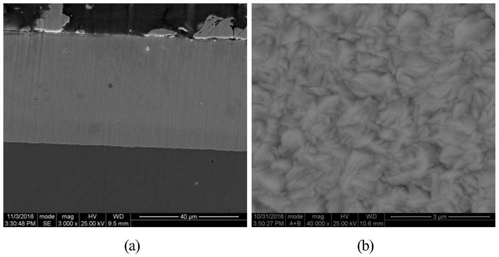
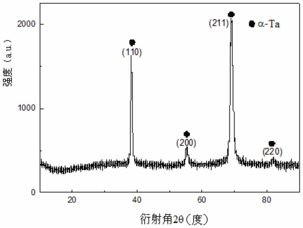
[0029] Observation of the cross-section and surface of the deposited tantalum coating shows that the structure of the film layer is dense and well combined with the substrate, such as figure 1 (a) and figure 1 (b) shown. X-ray diffraction analysis shows that the existence of almost no β-Ta diffraction peaks can be detected in the coating, all of which are the diffraction peaks of body...
Embodiment 2
[0031] The substrate is made of 25Cr3Mo3NiNb alloy steel. The sample size is 15mm×10mm×2mm. The purity of the tantalum target is 99.99wt%. chamber; the chamber is vacuumed to below 7×10 -2 Pa, turn on the heater, heat the surrounding of the sample to 300 degrees Celsius, and then pump the background vacuum to 7×10 -3 Pa. Inject argon to 1.3×10 -1 Pa, start sputtering. The power supply used is a DC power supply, the sputtering power is set to 2.0kW, and the sputtering power density is 4W / cm 2 , the deposition time is about 1 hour, and the thickness of the tantalum coating is about 12 μm.
[0032] Observation of the cross-section and surface of the deposited tantalum coating shows that the structure of the coating is dense and well combined with the substrate. X-ray diffraction analysis shows that the existence of almost no β-Ta diffraction peaks can be detected in the coating, all of which are the diffraction peaks of α-Ta, such as Figure 4 shown. The thermal shock resi...
Embodiment 3
[0034] The substrate is PCrNi3M O V alloy steel, the sample size is 15mm×10mm×2mm, the purity of the tantalum target is 99.99wt%, the distance between the substrate and the target is 25mm (in the range of the negative glow area), the substrate is loaded into the working room after surface cleaning; The studio is vacuumed to below 7×10 -2 Pa, turn on the heater, heat the surrounding of the sample to 270 degrees Celsius, and then pump the background vacuum to 7×10 -3 Pa. Inject argon to 1.2×10 -1 Pa, start sputtering. The power supply used is a DC power supply, the sputtering power is set to 2.0kW, and the sputtering power density is 4W / cm 2, the deposition time was about 6 hours, and the thickness of the tantalum coating was about 63 μm.
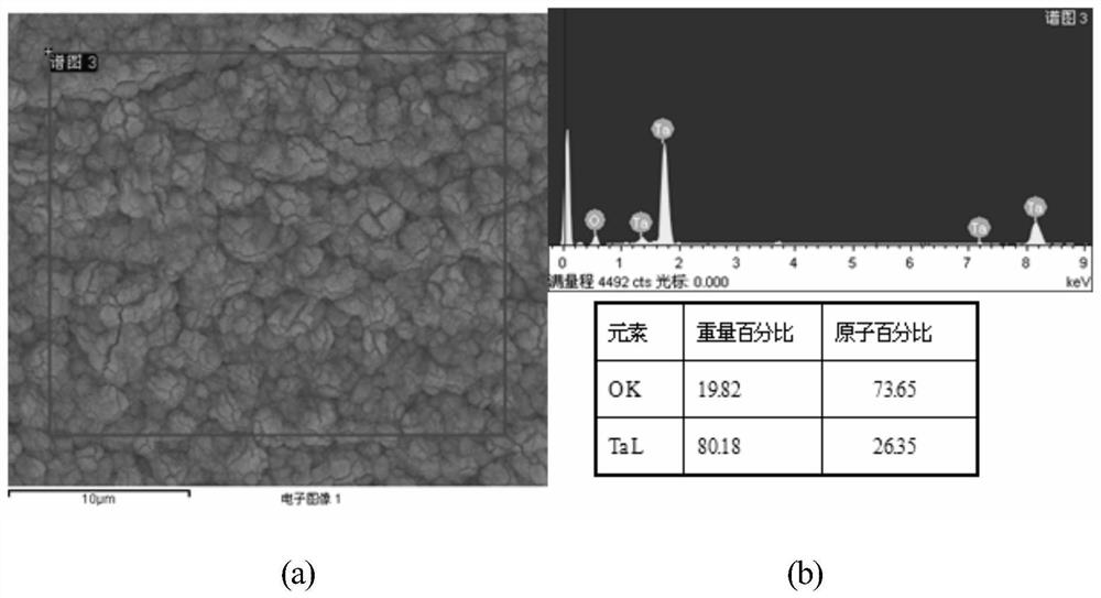
[0035] Observation of the cross-section and surface of the deposited tantalum coating shows that the structure of the coating is dense and well combined with the substrate. X-ray diffraction analysis shows that almost no β-Ta diffractio...
PUM
| Property | Measurement | Unit |
|---|---|---|
| thickness | aaaaa | aaaaa |
| melting point | aaaaa | aaaaa |
| thermal conductivity | aaaaa | aaaaa |
Abstract
Description
Claims
Application Information


