Method for preparing polycrystalline silicon thin film by laser crystallization and product and thin film transistor obtained

A polysilicon thin film, laser crystallization technology, applied in the manufacture of transistors, semiconductor devices, semiconductor/solid-state devices, etc., can solve the problems of uneven color, uneven film thickness of amorphous silicon, temperature fluctuation of amorphous silicon, etc.

Active Publication Date: 2018-06-15
TRULY HUIZHOU SMART DISPLAY
View PDF5 Cites 2 Cited by
  • Summary
  • Abstract
  • Description
  • Claims
  • Application Information

AI Technical Summary

Problems solved by technology

[0003] At present, the excimer laser tempering technology and metal-induced amorphous silicon crystallization are commonly used in the production of polysilicon thin films, namely ELA technology and MIA technology, but the existing ELA technology has the following defects: laser Energy fluctuations between different pulses, uneven energy density at different parts of the laser beam cross-section, uneven thickness of amorphous silicon film, etc., these defects will lead to temperature fluctuations and unevenness of amorphous silicon after being heated by laser, thus affecting the uniformity of crystallization Insufficient brightness of transistors, uneven color ELA mura and other problems

Method used


Image

  • Method for preparing polycrystalline silicon thin film by laser crystallization and product and thin film transistor obtained
  • Method for preparing polycrystalline silicon thin film by laser crystallization and product and thin film transistor obtained
  • Method for preparing polycrystalline silicon thin film by laser crystallization and product and thin film transistor obtained

Examples


Embodiment 1

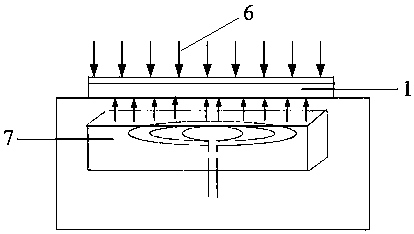
[0026] Embodiment 1: A method for preparing a polysilicon film by laser crystallization, the steps are:

[0027] S1, forming a thermistor layer on the glass substrate;

[0028] S2, forming an amorphous silicon layer on the thermistor layer;

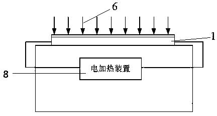
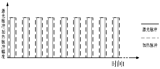
[0029] S3, irradiating the amorphous silicon film layer in the crystallization step S2 with laser pulses, and at the same time heating the thermistor layer by means of electric heating or electromagnetic heating, so that the amorphous silicon layer is converted into a polysilicon layer.

[0030] The thermistor layer is a negative temperature coefficient NTC resistance layer, and its constituent materials include metal oxides and non-oxides; the metal oxides are manganese, copper, silicon, cobalt, iron, nickel, zinc at least one of; said non-oxide is at least one of silicon carbide, tin selenide and tantalum nitride. The step S3 is to heat the thermistor layer by means of electric heating or electromagnetic heating.

[0031] like figur...

Embodiment 2

[0035] Embodiment 2: On the basis of Embodiment 1, the process of forming an isolation layer on the glass substrate is also included before the step S1, and the isolation layer is one or both of silicon oxide and silicon nitride. Before the step S2, a buffer layer is formed on the thermistor layer, and the buffer layer is one or both of silicon oxide and nitride. The isolation layer and the buffer layer are formed by PECVD; the thermistor layer is formed by PECVD or PVD or coating and sintering.

[0036] like Figure 5 As shown: the obtained polysilicon thin film includes an isolation layer 4 , a thermistor layer 2 , a buffer layer 5 and a polysilicon layer 3 formed on a glass substrate 1 in sequence. The polysilicon thin film has the characteristics of good crystal grain uniformity, good crystal grain density consistency, good crystal grain mobility and stability.

Embodiment 3

[0037] Embodiment 3: a thin film transistor comprising the polysilicon thin film described in Embodiment 1 or Embodiment 2. The thin film transistor has the characteristics of no spot, uniform brightness and good electrical performance.


PUM


Abstract

The invention relates to the technical field of TFT thin film transistors, in particular to a method for preparing a polycrystalline silicon thin film by laser crystallization and a product and a thinfilm transistor obtained. The preparation steps are as follows: S1, forming a thermistor layer on a glass substrate; S2, forming an amorphous silicon layer on the thermistor layer; and S3, irradiating the amorphous silicon film layer in S2 with laser pulse, and heating the thermistor layer by electric heating or electromagnetic heating to convert the amorphous silicon layer into a polycrystallinesilicon layer. There is a process of forming an isolation layer on the glass substrate before S1, and the isolation layer is made of silicon oxide and / or silicon nitride. The polycrystalline siliconthin film obtained has the characteristics of high grain uniformity, high consistency of grain density, high grain migration rate and high stability. The thin film transistor obtained has the characteristics of no spot, uniform brightness and good electrical performance.

Description

technical field [0001] The invention relates to the technical field of TFT thin film transistors, in particular to a method for preparing polysilicon thin films by laser crystallization, the obtained products and thin film transistors. Background technique [0002] Polysilicon has been widely valued in the manufacture of thin film transistors in recent years, especially in the application of thin film transistors to drive displays, due to its superior electrical properties to amorphous silicon and the advantages of lower cost than single crystal silicon. [0003] At present, the excimer laser tempering technology and metal-induced amorphous silicon crystallization are commonly used in the production of polysilicon thin films, namely ELA technology and MIA technology, but the existing ELA technology has the following defects: laser Energy fluctuations between different pulses, uneven energy density at different parts of the laser beam cross-section, uneven thickness of amorph...

Claims


Application Information

Patent Timeline
Patent Type & Authority Applications(China)
IPC IPC(8): H01L21/02H01L29/786
CPCH01L21/02422H01L21/02491H01L21/02532H01L21/02667H01L21/02686H01L29/78672
Inventor 陈卓徐先新张鑫磊任思雨苏君海李建华
Owner TRULY HUIZHOU SMART DISPLAY
Why Eureka
Try Eureka