

Additive-doped perovskite film and preparation method and application thereof
An additive and perovskite technology, which is applied in semiconductor/solid-state device manufacturing, electrical components, electric solid-state devices, etc., can solve the problems of not being able to inhibit the movement of iodine ions, and not being able to prevent the aging of perovskite materials, so as to promote industrial production, Improved long-term stability and extended service life
- Summary
- Abstract
- Description
- Claims
- Application Information
AI Technical Summary
Problems solved by technology
Method used
Image

Examples
preparation example Construction
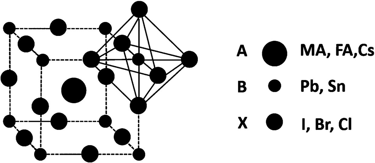
[0049] Since during the preparation of perovskite thin films, iodine vacancies will be generated locally, and the existence of iodine vacancies will promote the migration of iodine ions in perovskite. Therefore, the introduction of additives to promote the uniform distribution of iodine can effectively reduce iodine vacancies. Generally, metal halides with smaller radius, such as potassium iodide, can effectively reduce the concentration of iodine vacancies in perovskite. Therefore, the use of the additives disclosed in the present invention can inhibit iodide ion migration, thereby improving the long-term stability of perovskite cells.
[0050] In the above embodiments, the additive MG is incorporated into the perovskite film by solution mixing, co-evaporation, anti-solvent or lamination.
[0051] The present invention also discloses a method for preparing the additive-doped perovskite film as described above, comprising the following steps:
[0052] Step S11, preparing a pe...
example 1
[0078] Example 1, a method for preparing a perovskite solar cell.
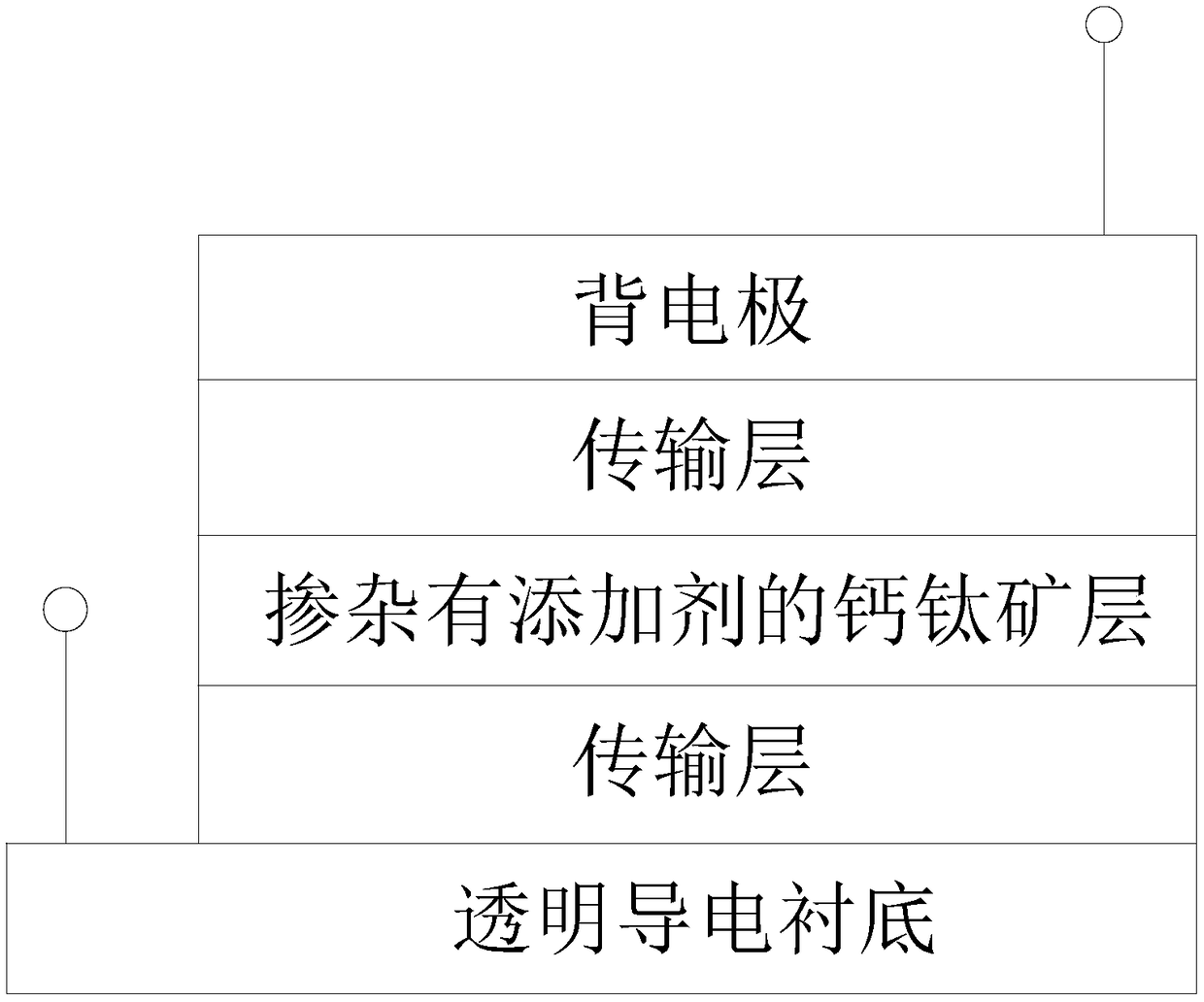
[0079] Please refer to the attached figure 2 The schematic diagram of the internal structure of the perovskite solar cell shown includes the following steps:
[0080] (1) Clean a 5×5cm ITO glass plate with detergent, deionized water, acetone, and isopropanol for 30 minutes, and then use N 2 After drying, it was treated with UV O-zone for 10 minutes;
[0081] (2) Preparation of NiO thin film as electron transport layer;
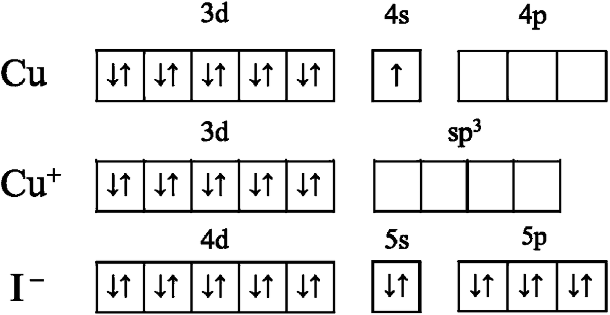
[0082] (3) Preparation of doped or modified metal halide precursor: 461 mg of PbI 2 (1mmol), 19.05mg cuprous iodide CuI (0.1mmol) were dissolved in 1mL DMF solution, heated and stirred at 60°C for 2h, added 20uL chlorobenzene, mixed completely and set aside;
[0083] (4) Preparation of doped PbI by slot coating using the prepared precursor solution 2 film;
[0084] (5) Place the prepared metal halide film in the film forming cavity, and use a vacuum pump to control the air pressure at 1...
Embodiment 2
[0089] (1) Clean a 10×10cm FTO glass plate with detergent, deionized water, acetone, and isopropanol for 30 minutes, and then use N 2 After drying, it was treated with UV O-zone for 10 minutes;
[0090] (2) Preparation of CuSCN film as a hole transport layer;
[0091] (3) Preparation of perovskite solution with additives: 461 mg of PbI 2 (1mmol), 159mg of MAI (1mmol) were dissolved in 1mL of DMF solution, 68uL of anhydrous DMSO was added, and 36.9mg of cuprous bromide CuBr was added as an additive, heated and stirred at 70°C for 2h, mixed completely before use;
[0092] (4) Use the doped perovskite solution to prepare the perovskite film doped with stabilizer by slit coating, and anneal at 60~150°C for 10~120min, with a thickness of 200~600nm;
[0093] (5) Re-deposit the electron transport layer ZnO on the substrate, with a thickness of 20~50nm;
[0094] (6) Evaporate metal conductive layer Au electrodes to prepare perovskite solar cells.
PUM
 Abstract
Description
Claims
Application Information