Deep-ultraviolet detector based on lead-free double-perovskite film, and preparation method

A lead-free double perovskite, deep ultraviolet light technology, used in semiconductor/solid-state device manufacturing, photovoltaic power generation, electric solid-state devices, etc., can solve the problems of structural instability and lead toxicity, and achieve excellent performance and environmental friendliness. , the effect of simple preparation process

Active Publication Date: 2018-08-14
ZHENGZHOU UNIV
View PDF10 Cites 18 Cited by
  • Summary
  • Abstract
  • Description
  • Claims
  • Application Information

AI Technical Summary

Problems solved by technology

[0003] At present, the reported perovskite-based photodetectors are mainly organic-inorganic hybrid perovskite material systems (CH 3 NH 3 wxya 3 , X=Cl/Br/I), but the wide application of this type of material faces

Method used


Image

  • Deep-ultraviolet detector based on lead-free double-perovskite film, and preparation method
  • Deep-ultraviolet detector based on lead-free double-perovskite film, and preparation method
  • Deep-ultraviolet detector based on lead-free double-perovskite film, and preparation method

Examples


Embodiment 1

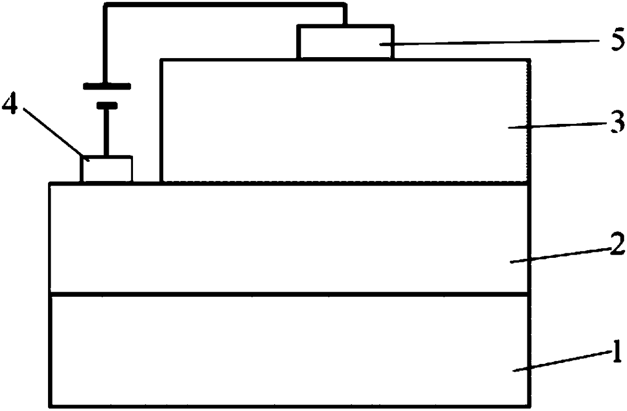
[0032] (1) cleaning substrate 1, the adopted substrate is double-sided polished Al 2 O 3 substrate.

[0033] Al with double throw 2 O 3 A single wafer is used as the substrate 1, and it is chemically cleaned. The cleaning steps are: put the substrate in acetone and ethanol solutions for ultrasonic cleaning for 5 minutes, and then recirculate once; Blow dry with nitrogen for later use.

[0034] (2) An n-type electron supply layer 2 is prepared.

[0035] Double-throw Al by RF magnetron sputtering 2 O 3 The deposition of the ZnO electron supply layer is completed on the substrate 1, and the specific steps are: install ZnO:Al 2 O 3 (mass fraction: Al 2 O 3: ZnO=1.2:98.8%) ceramic target, adjust the distance between the target and the substrate to 10 cm; turn on the mechanical pump, vacuumize the cavity, when the vacuum of the cavity is lower than 10 Pascals, turn on the molecular The pump continues to evacuate until the cavity vacuum is lower than 2.0×10 -3 Pascal; fee...

Embodiment 2

[0044] (1) cleaning substrate 1, the adopted substrate is double-sided polished Al 2 O 3 substrate.

[0045] In this embodiment, double-throwing Al 2 O 3 The cleaning method is the same as in Example 1.

[0046] (2) The n-type electron supply layer 2 is prepared, and a GaN semiconductor material is used as the electron supply layer.

[0047] A double-throw Al 2 O 3 The epitaxial growth of the GaN electron transport layer 2 is completed on the substrate 1 . The specific growth process is as follows: the cleaned double-polished Al 2 O 3 The substrate 1 is placed in the reaction chamber; then, the sample is heated to 1060°C, and hydrogen gas (100 sccm) is introduced into the Al 2 O 3 The surface of the substrate 1 is subjected to high-temperature treatment to remove impurities on the surface; then, the temperature of the sample is lowered to 550° C. to grow a GaN low-temperature nucleation layer with a thickness of 30 nanometers; and the temperature is raised to 1035° C...


PUM

PropertyMeasurementUnit
Thicknessaaaaaaaaaa
Thicknessaaaaaaaaaa
Electron concentrationaaaaaaaaaa

Abstract

The invention belongs to the technical field of the semiconductor photoelectric detection, and specifically relates to a deep-ultraviolet detector based on a lead-free double-perovskite film, and a preparation. The structure is composed of a double-side polished Al2O3 substrate, n-type bandwidth gap electronic transmission layer, a Cs2AgBiBr6 light absorption layer and a contact electrode. On theone hand, the instability and the lead positioning and like adverse factors of the traditional perovskite structure are overcome; on the other hand, the fast separation and transmission of the photo-generated carrier can be realized by means of the energy band matching between the bandwidth gap electronic transmission layer and the Cs2AgBiBr6 light absorption layer, and the light detection range of the device can be extended to the deep ultraviolet region from the visible light. The preparation method of the device disclosed by the invention is simple and practical, and environment-friendly; the prepared photoelectric detector has high detection rate and response speed, and has very important application value.

Description

technical field [0001] The invention belongs to the technical field of semiconductor photoelectric detection, and in particular relates to a deep ultraviolet photodetector based on a lead-free double perovskite film and a preparation method thereof. Background technique [0002] Metal halide perovskites with the general formula ABX 3 , wherein A is methylammonium (MA), formamidine (FA) or Cs, B is Pb or Sn, etc., and X is Cl, Br or I. In recent years, new solar cells based on lead halide perovskite materials have attracted widespread attention, and have shown high conversion efficiencies greater than 22% in a short period of time, which is mainly due to the large light absorption coefficient of the material, It has excellent characteristics such as high carrier transport rate, simple preparation process, and its bandwidth is continuously adjustable in the visible light region. With the further understanding of this material, the research field based on perovskite has begun...

Claims


Application Information

Patent Timeline
IPC IPC(8): H01L51/42
CPCH10K30/152H10K30/151H10K30/00Y02E10/549Y02P70/50
Inventor 史志锋李营雷玲芝马壮壮陈磊磊李新建
Owner ZHENGZHOU UNIV
Why Eureka
Try Eureka