A semiconductor material laser electrochemical composite micromachining method and device

A semiconductor and electrochemical technology, which is applied in the field of laser electrochemical composite micromachining and devices for semiconductor materials, can solve problems such as unavailable technical literature, achieve the elimination of recasting layer and residual stress, good surface quality, and reduce laser heat damage effect

Active Publication Date: 2020-07-31
JIANGSU UNIV
View PDF6 Cites 0 Cited by
  • Summary
  • Abstract
  • Description
  • Claims
  • Application Information

AI Technical Summary

Problems solved by technology

But no relevant technical literature was found

Method used


Image

  • A semiconductor material laser electrochemical composite micromachining method and device
  • A semiconductor material laser electrochemical composite micromachining method and device

Examples


Embodiment 1

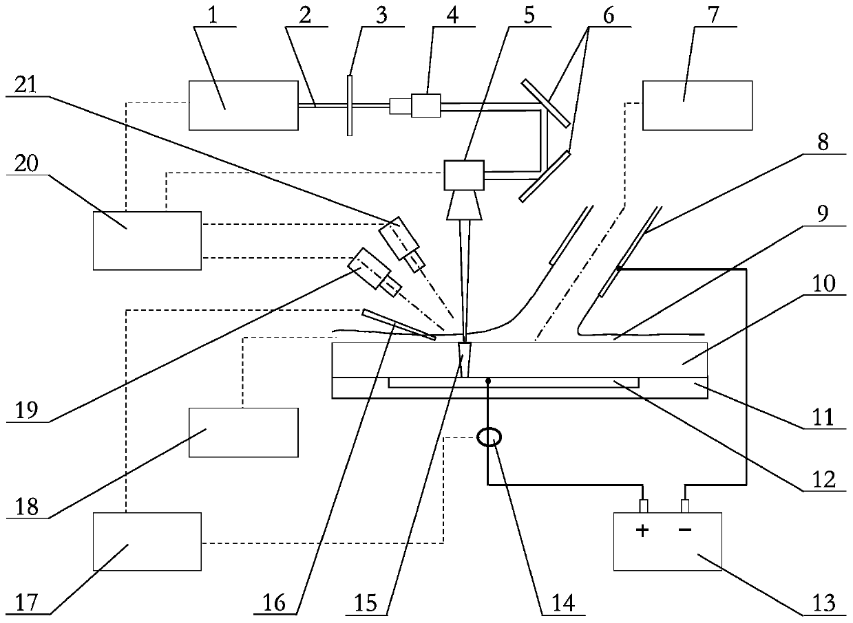
[0033] Embodiment 1: This embodiment is a semiconductor material laser electrolytic composite processing method based on a localized conductive channel. The laser beam 2 generated by the laser 1 is adjusted and transmitted by an external optical path and then focused on the surface of the semiconductor material 10, and the thermal effect of the laser is used to process high-efficiency materials. Removal, complete micro-hole, micro-groove processing. At the same time, the thermal effect of the laser generates a local temperature field around the microholes, which locally enhances the conductivity of semiconductor materials such as single crystal silicon. On this basis, the stable low-voltage electrolyte beam generation and adjustment device is used to introduce a biased electrolyte beam, and in the region where the conductivity is enhanced around the laser irradiation area, electrochemical anodic dissolution is introduced locally, which can effectively eliminate the recast layer...

Embodiment 2

[0035] Embodiment 2: in combination with figure 1 , the present embodiment is a semiconductor material laser electrolytic composite processing system based on a localized conductive channel, including an optical path system, a stable low-pressure jet generation and adjustment system, and an electrolytic processing system; the optical path system includes a laser 1 and an external optical path, wherein the external optical path includes an optical gate 3. Beam expander 4, vibrating mirror 5 and mirror 6. The laser 1 outputs the laser beam 2, passes through the shutter 3 of the protection device, expands the diameter of the laser beam by the beam expander 4, adjusts the direction through the reflector 6, and finally controls the movement form of the beam by the vibrating mirror 5, irradiates the surface of the semiconductor material 10, and A localized conductive channel 15 is formed within the semiconductor material 10 . Both the generation of the laser beam 2 and the movement...

Embodiment 3

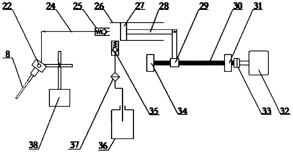
[0040] Embodiment 3: in combination with figure 2 , the embodiment is a stable low-pressure jet flow generation and adjustment system, including a servo motor 32 driving a ball screw 30 to rotate through a coupling 33, and the two ends of the ball screw 30 are supported by a first support seat 31 and a second support seat 34; The slider 29 matched with the ball screw 30 converts the rotation of the ball screw 30 into the linear motion of the piston rod 28 , thereby pushing the electrolyte in the electrolyte cylinder 26 to output at a constant speed. The electrolyte flows into the metal needle 8 through the first one-way valve 25 and the hose 24 to form a stable low-pressure jet. The angle of the low-pressure jet can be adjusted by the angle regulator 22 , and the impact position of the jet can be adjusted by the XYZ three-way fine-tuning platform 38 . The first one-way valve 25 and the second one-way valve 35 can cooperate with the forward and reverse movement of the ball sc...


PUM

PropertyMeasurementUnit
electrical conductivityaaaaaaaaaa

Abstract

The invention discloses a laser electrochemical compound micromachining method and device for a semiconductor material, and belongs to the field of special machining. The method comprises the steps that the semiconductor material is heated with laser beams through the characteristic that the electric conductivity of the semiconductor material such as monocrystalline silicon is significantly increased along with increasing of the temperature, the electric conduction property of the material near a machining area is locally enhanced, an electric conduction channel that currents pass preferentially is formed, on this basis, electrolytic machining is introduced in a bias electro-hydraulic beam mode, laser electrochemical self-coupling combined machining near the machining area is achieved, tool setting is not needed, therefore, it is guaranteed that no surface residue adhesion occurs in the laser machining process, the cooling effect can be strengthened, and the purposes of reducing heat damage and residual stress and improving the machining surface quality are achieved. The device comprises a laser, an external light path, an electrolytic power supply and a stable jet flow generatingdevice. The device can generate stable low-voltage electrolytic solution jet flow and achieve impact angle and position adjustment, and it is guaranteed that precise adjustment of the relative positions between the laser beams and the impact jet flow is achieved.

Description

technical field [0001] The invention relates to a processing method and device for processing structures such as micro-slits, holes, and grooves in the field of special processing, and in particular to a laser electrolytic composite processing method realized by utilizing the temperature sensitivity of the conductivity of semiconductor materials such as single crystal silicon and the like. device. Background technique [0002] Semiconductor materials represented by silicon and germanium have good structural and functional properties, and are widely used in chips, photovoltaics, medical devices, micro-electromechanical systems and other fields. Processing microstructures with specific morphology on the surface of semiconductor materials can achieve multiple functions, for example: submicron-scale periodic microgroove structure can enhance the anti-reflection performance of the material surface; honeycomb densely distributed smooth micropit groups can form microconcave lenses ...

Claims


Application Information

Patent Timeline
Patent Type & Authority Patents(China)
IPC IPC(8): B23H5/06B23K26/402
CPCB23H5/06B23K26/402
Inventor 朱浩张朝阳徐坤顾秦铭朱帅杰赵斗艳
Owner JIANGSU UNIV
Why Eureka
Try Eureka